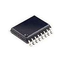
HV450WG Supertex, HV450WG Datasheet - Page 3

HV450WG
Manufacturer Part Number
HV450WG
Description
Telephone Ringers SO-16 HV RING GEN
Manufacturer
Supertex
Type
Multipler
Datasheet
1.HV450DB1.pdf
(4 pages)
Specifications of HV450WG
Function
Telecom Ringer
Mounting Style
SMD/SMT
Product
Telecom Ringer
Package / Case
SOIC-16 Wide
Maximum Operating Temperature
+ 85 C
Minimum Operating Temperature
- 40 C
Primary Target Application
Generator Circuit
Lead Free Status / RoHS Status
Lead free / RoHS Compliant
Block Diagram
Pin Description
V
V
V
V
GND
P
P
N
EN
Mode
HV
V
V
P
N
PP
NN1
NN2
DD
GND
IN
IN
psen
nsen
gate
gate
OUT
P-channel gate voltage supply. Generated by an internal linear regulator. A 0.1µF capacitor should be connected between
P
Negative high voltage supply.
N-channel gate voltage supply. Generated by an internal linear regulator. A 0.1µF capacitor should be connected between
V
Logic supply voltage.
Low voltage ground.
High voltage power ground.
Logic control input. When mode is high, logic input high turns OFF output high voltage P-Channel.
Logic control input. When mode is high, logic input high turns ON output high voltage N-Channel.
Logic enable input. Logic low enables IC.
Logic mode input. Logic low activates 200nsec deadband. When mode is low, N
P-Channels. Pin is not used and should be connected to V
High voltage output. Voltage swings from P
Pulse by pulse over current sensing for P-Channel MOSFET.
Pulse by pulse over current sensing for N-Channel MOSFET.
Gate drive for external P-channel MOSFET.
Gate drive for external N-channel MOSFET.
GND
NN2
and V
and V
Mode
GND
V
N
P
EN
DD
IN
IN
NN1
PP
.
.
Logic
GND
Translator
Translator
Voltage
Voltage
to V
Level
Level
High
High
NN1
.
3
DD
Linear
Linear
V
Reg
Reg
DD
or ground.
Current
Current
Sense
Sense
Driver
Driver
and
and
IN
turns on and off the high voltage N- and
V
P
V
HV
P
N
V
V
V
psen
gate
PP
GND
gate
nsen
NN1
NN2
OUT


