SIHG22N60S-E3 Vishay, SIHG22N60S-E3 Datasheet - Page 6
SIHG22N60S-E3
Manufacturer Part Number
SIHG22N60S-E3
Description
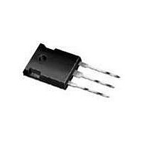
MOSFET N-CH 600V 22A TO247
Manufacturer
Vishay
Datasheet
1.SIHG22N60S-E3.pdf
(7 pages)
Specifications of SIHG22N60S-E3
Transistor Polarity
N-Channel
Fet Type
MOSFET N-Channel, Metal Oxide
Fet Feature
Standard
Rds On (max) @ Id, Vgs
190 mOhm @ 22A, 10V
Drain To Source Voltage (vdss)
600V
Current - Continuous Drain (id) @ 25° C
22A
Vgs(th) (max) @ Id
4V @ 250µA
Gate Charge (qg) @ Vgs
75nC @ 10V
Input Capacitance (ciss) @ Vds
2810pF @ 25V
Power - Max
250W
Mounting Type
Through Hole
Package / Case
TO-247-3 (Straight Leads)
Forward Transconductance Gfs (max / Min)
9.4 S
Gate Charge Qg
75 nC
Mounting Style
Through Hole
Resistance Drain-source Rds (on)
0.16 Ohms
Drain-source Breakdown Voltage
600 V
Gate-source Breakdown Voltage
20 V
Continuous Drain Current
22 A
Power Dissipation
250 W
Continuous Drain Current Id
22A
Drain Source Voltage Vds
600V
On Resistance Rds(on)
160mohm
Rds(on) Test Voltage Vgs
10V
Threshold Voltage Vgs Typ
4V
Operating Temperature Range
-55°C To +150°C
Transistor Case Style
TO-247
Rohs Compliant
Yes
Lead Free Status / RoHS Status
Lead free / RoHS Compliant
Lead Free Status / RoHS Status
Lead free / RoHS Compliant, Lead free / RoHS Compliant
Available stocks
Company
Part Number
Manufacturer
Quantity
Price

Part Number:
SIHG22N60S-E3
Manufacturer:
VISHAY/威世
Quantity:
20 000


SiHG22N60S
Vishay Siliconix
Vishay Siliconix maintains worldwide manufacturing capability. Products may be manufactured at one of several qualified locations. Reliability data for Silicon
Technology and Package Reliability represent a composite of all qualified locations. For related documents such as package/tape drawings, part marking, and
reliability data, see www.vishay.com/ppg?91393.
www.vishay.com
6
THE PRODUCT DESCRIBED HEREIN AND THIS DATASHEET ARE SUBJECT TO SPECIFIC DISCLAIMERS, SET FORTH AT
V
Fig. 13a - Basic Gate Charge Waveform
GS
V
G
Q
GS
Charge
Q
Q
GD
G
Re-applied
voltage
Rever e
recovery
current
+
R
-
g
This datasheet is subject to change without notice.
D.U.T.
Note
a. V
Driver gate drive
D.U.T. l
D.U.T. V
Inductor current
= 5 V for logic level device
P.W.
D
D
waveform
waveform
Fig. 14 - For N-Channel
Peak Diode Recovery dV/dt Test Circuit
Ripple ≤ 5 %
Body diode forward drop
Period
Body diode forward
+
-
• dV/dt controlled by R
• Driver ame type a D.U.T.
• I
• D.U.T. - device under te t
Diode recovery
current
D
controlled by duty factor “D”
Circuit layout con ideration
dV/dt
• Low tray inductance
•
• Low leakage inductance
current tran former
dI/dt
round plane
D =
-
g
Period
P.W.
12 V
+
Fig. 13b - Gate Charge Test Circuit
V
GS
Same type as D.U.T.
Current regulator
V
I
V
DD
D
0.2 µF
= 10 V
+
-
V
DD
a
Current sampling resistors
3 mA
50 kΩ
0.3 µF
I
G
www.vishay.com/doc?91000
S11-0440-Rev. D, 14-Mar-11
Document Number: 91393
D.U.T.
I
D
+
-
V
DS
Related parts for SIHG22N60S-E3
Image
Part Number
Description
Manufacturer
Datasheet
Request
R

Part Number:
Description:
357-036-542-201 CARDEDGE 36POS DL .156 BLK LOPRO
Manufacturer:
Vishay
Datasheet:
Part Number:
Description:
357-036-542-201 CARDEDGE 36POS DL .156 BLK LOPRO
Manufacturer:
Vishay
Datasheet:
Part Number:
Description:
357-036-542-201 CARDEDGE 36POS DL .156 BLK LOPRO
Manufacturer:
Vishay
Datasheet:
Part Number:
Description:
357-036-542-201 CARDEDGE 36POS DL .156 BLK LOPRO
Manufacturer:
Vishay
Datasheet:
Part Number:
Description:
357-036-542-201 CARDEDGE 36POS DL .156 BLK LOPRO
Manufacturer:
Vishay
Datasheet:
Part Number:
Description:
357-036-542-201 CARDEDGE 36POS DL .156 BLK LOPRO
Manufacturer:
Vishay
Datasheet:
Part Number:
Description:
357-036-542-201 CARDEDGE 36POS DL .156 BLK LOPRO
Manufacturer:
Vishay
Datasheet:
Part Number:
Description:
357-036-542-201 CARDEDGE 36POS DL .156 BLK LOPRO
Manufacturer:
Vishay
Datasheet:
Part Number:
Description:
357-036-542-201 CARDEDGE 36POS DL .156 BLK LOPRO
Manufacturer:
Vishay
Datasheet:
Part Number:
Description:
357-036-542-201 CARDEDGE 36POS DL .156 BLK LOPRO
Manufacturer:
Vishay
Datasheet:
Part Number:
Description:
357-036-542-201 CARDEDGE 36POS DL .156 BLK LOPRO
Manufacturer:
Vishay
Datasheet:
Part Number:
Description:
357-036-542-201 CARDEDGE 36POS DL .156 BLK LOPRO
Manufacturer:
Vishay
Datasheet:
Part Number:
Description:
357-036-542-201 CARDEDGE 36POS DL .156 BLK LOPRO
Manufacturer:
Vishay
Datasheet:
Part Number:
Description:
357-036-542-201 CARDEDGE 36POS DL .156 BLK LOPRO
Manufacturer:
Vishay
Datasheet:
Part Number:
Description:
357-036-542-201 CARDEDGE 36POS DL .156 BLK LOPRO
Manufacturer:
Vishay
Datasheet: