IRF7322D1TRPBF International Rectifier, IRF7322D1TRPBF Datasheet
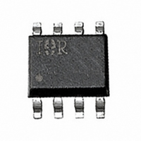
MOSFET P-CH 20V 5.3A 8-SOIC

IRF7322D1TRPBF

Manufacturer Part Number
IRF7322D1TRPBF
Description
MOSFET P-CH 20V 5.3A 8-SOIC
Manufacturer
International Rectifier
Series
FETKY™r
Datasheet

Specifications of IRF7322D1TRPBF

Fet Type
MOSFET P-Channel, Metal Oxide
Fet Feature
Diode (Isolated)
Rds On (max) @ Id, Vgs
62 mOhm @ 2.9A, 4.5V
Drain To Source Voltage (vdss)
20V
Current - Continuous Drain (id) @ 25° C
5.3A
Vgs(th) (max) @ Id
700mV @ 250µA
Gate Charge (qg) @ Vgs
29nC @ 4.5V
Input Capacitance (ciss) @ Vds
780pF @ 15V
Power - Max
2W
Mounting Type
Surface Mount
Package / Case
8-SOIC (3.9mm Width)
Transistor Polarity
P-Channel
Resistance Drain-source Rds (on)
62 mOhms
Drain-source Breakdown Voltage
- 20 V
Gate-source Breakdown Voltage
12 V
Continuous Drain Current
- 5.3 A
Power Dissipation
2 W
Mounting Style
SMD/SMT
Gate Charge Qg
19 nC
Lead Free Status / RoHS Status
Lead free / RoHS Compliant
Other names
IRF7322D1PBFTR
IRF7322D1TRPBF
IRF7322D1TRPBFTR

Available stocks

Company
Part Number
Manufacturer
Quantity
Price
Part Number:
IRF7322D1TRPBF
Manufacturer:
GOODSKY
Quantity:
3 000
Company:
Part Number:
IRF7322D1TRPBF
Quantity:
8 421
Description
Absolute Maximum Ratings (T
Thermal Resistance Ratings
Notes:
À
Á
Â
Ã
www.irf.com
l
The FETKY family of co-packaged MOSFETs and Schottky diodes offers the
designer an innovative, board space saving solution for switching regulator
and power management applications. Generation 5 HEXFET Power
MOSFETs utilize advanced processing techniques to achieve extremely low
on-resistance per silicon area. Combinining this technology with
International Rectifier's low forward drop Schottky rectifiers results in an
extremely efficient device suitable for use in a wide variety of portable
electronics applications.
The SO-8 has been modified through a customized leadframe for
enhanced thermal characteristics. The SO-8 package is designed for vapor
phase, infrared or wave soldering techniques.
l
l
l
l
l
l
Parameter
R
Parameter
I
I
I
P
P
V
dv/dt
T
D
D
DM
θJA
D
D
GS
J,
Repetitive rating; pulse width limited by maximum junction temperature (see figure 9)
I
Pulse width ≤ 300µs; duty cycle ≤ 2%
Surface mounted on FR-4 board, t ≤ 10sec
Lead-Free
Co-packaged HEXFET
and Schottky Diode
Ideal For Buck Regulator Applications
P-Channel HEXFET
Low V
Generation 5 Technology
SO-8 Footprint
@ T
@ T
SD
T
@T
@T
STG
≤ -2.9A, di/dt ≤ -77A/µs, V
A
A
A
A
= 25°C
= 70°C
= 25°C
= 70°C
F
Schottky Rectifier
Continuous Drain Current, V
Pulsed Drain Current À
Power Dissipation
Linear Derating Factor
Gate-to-Source Voltage
Peak Diode Recovery dv/dt Á
Junction and Storage Temperature Range
Junction-to-Ambient
DD
®
≤ V
Power MOSFET
(BR)DSS
A
, T
= 25°C unless otherwise noted)
J
≤ 150°C
Ã
GS
@ -4.5V
A
S
G
A
FETKY
1
2
3
4
Top View
IRF7322D1PbF
ä
MOSFET / Schottky Diode
8
7
6
5
-55 to +150
Maximum
K
K
D
D
± 12
Maximum
-5.3
-4.3
-5.0
-43
2.0
1.3
16
62.5
Schottky Vf = 0.39V
R
DS(on)
V
DSS
SO-8
PD - 95298
= 0.058Ω
= -20V
Units
mW/°C
°C/W
Units
V/ns
°C
W
V
A
1
10/12/04

Related parts for IRF7322D1TRPBF

IRF7322D1TRPBF Summary of contents

Page 1

... Generation 5 HEXFET Power MOSFETs utilize advanced processing techniques to achieve extremely low on-resistance per silicon area. Combinining this technology with International Rectifier's low forward drop Schottky rectifiers results in an extremely efficient device suitable for use in a wide variety of portable electronics applications. ...

Page 2

IRF7322D1PbF MOSFET Electrical Characteristics @ T Parameter V Drain-to-Source Breakdown Voltage (BR)DSS R Static Drain-to-Source On-Resistance DS(on) V Gate Threshold Voltage GS(th) g Forward Transconductance fs I Drain-to-Source Leakage Current DSS I Gate-to-Source Forward Leakage GSS Gate-to-Source Reverse Leakage Q ...

Page 3

VGS TOP -7.50V -4.50V -4.00V -3.50V -3.00V -2.70V -2.00V BOTTOM -1.50V 10 1 0.1 0 Drain-to-Source Voltage (V) DS 100 ° 1.5 2.0 2.5 3 Gate-to-Source Voltage ...

Page 4

IRF7322D1PbF 1400 1MHz iss 1200 rss oss ds gd 1000 C iss 800 C oss 600 400 C ...

Page 5

SINGLE PULSE (THERMAL RESPONSE) 0.1 0.00001 0.0001 0.001 Fig 9. Maximum Effective Transient Thermal Impedance, Junction-to-Ambient 0.8 0 0.4 0.2 0 Drain Current (A) ...

Page 6

IRF7322D1PbF Schottky Diode Characteristics 10 1 0.1 0.0 0.2 0.4 0.6 Forward Voltage Drop - V Forward Voltage Drop - 150° 125°C J ...

Page 7

SO-8 (Fetky) Package Outline 0.25 [.010 NOTES : 1. DIMENS IONING & T OLERANCING PER AS ME Y14.5M-1994. 2. CONTROLLING DIMENS ION: MILLIME ...

Page 8

IRF7322D1PbF SO-8 Tape and Reel Dimensions are shown in milimeters (inches) NOTES: 1. CONTROLLING DIMENSION : MILLIMETER. 2. ALL DIMENSIONS ARE SHOWN IN MILLIMETERS(INCHES). 3. OUTLINE CONFORMS TO EIA-481 & EIA-541. NOTES : 1. CONTROLLING DIMENSION : MILLIMETER. 2. OUTLINE ...

Related keywords