STP45NF06 STMicroelectronics, STP45NF06 Datasheet
STP45NF06
Specifications of STP45NF06
Available stocks


Related parts for STP45NF06


STP45NF06 Summary of contents
Page 1
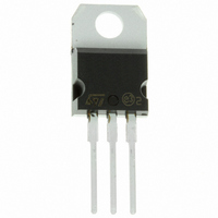
... STB45NF06 July 2010 N-channel 60 V, 0.023 Ω TO-220, D STripFET R I DS(on) D <0.028 Ω <0.028 Ω Figure 1. Marking P45NF06 B45NF06 Doc ID 7433 Rev 5 STB45NF06 STP45NF06 TM II Power MOSFET TO-220 D PAK Internal schematic diagram Package Packaging TO-220 Tube 2 D PAK Tape and reel ...
Page 2
... Contents Contents 1 Electrical ratings . . . . . . . . . . . . . . . . . . . . . . . . . . . . . . . . . . . . . . . . . . . . 3 2 Electrical characteristics . . . . . . . . . . . . . . . . . . . . . . . . . . . . . . . . . . . . . 4 2.1 Electrical characteristics (curves) 3 Test circuits 4 Package mechanical data . . . . . . . . . . . . . . . . . . . . . . . . . . . . . . . . . . . . . 9 5 Packaging mechanical data . . . . . . . . . . . . . . . . . . . . . . . . . . . . . . . . . . 12 6 Revision history . . . . . . . . . . . . . . . . . . . . . . . . . . . . . . . . . . . . . . . . . . . 14 2/ Doc ID 7433 Rev 5 STB45NF06, STP45NF06 ...
Page 3
... STB45NF06, STP45NF06 1 Electrical ratings Table 2. Absolute maximum ratings Symbol V Drain-source voltage ( Gate-source voltage GS I Drain current (continuous Drain current (continuous (1) I Drain current (pulsed Total dissipation at T TOT Derating factor (2) dv/dt Peak diode recovery voltage slope T Operating junction temperature J T Storage temperature stg 1 ...
Page 4
... I DS D(on =25V , f=1 MHz 10V GS Parameter Test conditions V = =4.7 Ω (see Figure 13) V =30V =4.7 Ω (see Figure 13) Doc ID 7433 Rev 5 STB45NF06, STP45NF06 Min. Typ 250µ 19A 0.023 0.028 D Min. Typ DS(on)max 920 - 225 6.5 14.5 Min. Typ. = =17 A, ...
Page 5
... STB45NF06, STP45NF06 Table 8. Source drain diode Symbol I Source-drain current SD (1) Source-drain current (pulsed) I SDM (2) Forward on voltage Reverse recovery time rr Q Reverse recovery charge rr Reverse recovery current I RRM 1. Pulsed: pulse duration=300µs, duty cycle 1.5% 2. Pulse width limited by safe operating area. Parameter ...
Page 6
... Electrical characteristics 2.1 Electrical characteristics (curves) Figure 2. Safe operating area Figure 4. Output characteristics Figure 6. Normalized breakdown voltage vs. temperature 6/15 Figure 3. Thermal impedance Figure 5. Transfer characteristics Figure 7. Static drain-source on resistance Doc ID 7433 Rev 5 STB45NF06, STP45NF06 ...
Page 7
... STB45NF06, STP45NF06 Figure 8. Gate charge vs. gate-source voltage Figure 10. Normalized gate threshold voltage vs. temperature Figure 12. Source-drain diode forward characteristics Figure 9. Capacitance variations Figure 11. Normalized on resistance vs. temperature Doc ID 7433 Rev 5 Electrical characteristics 7/15 ...
Page 8
... Figure 13. Switching times test circuit for resistive load Figure 15. Test circuit for inductive load switching and diode recovery times Figure 17. Unclamped inductive waveform 8/15 Figure 14. Gate charge test circuit Figure 16. Unclamped Inductive load test circuit Figure 18. Switching time waveform Doc ID 7433 Rev 5 STB45NF06, STP45NF06 ...
Page 9
... STB45NF06, STP45NF06 4 Package mechanical data In order to meet environmental requirements, ST offers these devices in different grades of ® ECOPACK packages, depending on their level of environmental compliance. ECOPACK specifications, grade definitions and product status are available at: www.st.com. ECOPACK trademark. Doc ID 7433 Rev 5 Package mechanical data ® ...
Page 10
... Doc ID 7433 Rev 5 STB45NF06, STP45NF06 inch MIN. TYP. MAX. 0.173 0.181 0.024 0.034 0.045 0.066 0.019 0.027 0.60 0.620 0.393 0.409 0.094 0.106 0.194 0.202 ...
Page 11
... STB45NF06, STP45NF06 DIM PAK MECHANICAL DATA TO-247 MECHANICAL DATA mm. MIN. TYP MAX. 4.4 4.6 2.49 2.69 0.03 0.23 0.7 0.93 1.14 1.7 0.45 0.6 1.23 1.36 8.95 9. 10.4 8.5 4.88 5.28 15 15.85 1.27 1.4 1.4 1.75 2.4 3.2 0.4 0º 4º ...
Page 12
... Doc ID 7433 Rev 5 STB45NF06, STP45NF06 REEL MECHANICAL DATA mm inch DIM. MIN. MAX. MIN. MAX. A 330 12.992 B 1.5 0.059 C 12 ...
Page 13
... STB45NF06, STP45NF06 DIM PAK MECHANICAL DATA TO-247 MECHANICAL DATA mm. MIN. TYP MAX. 4.4 4.6 2.49 2.69 0.03 0.23 0.7 0.93 1.14 1.7 0.45 0.6 1.23 1.36 8.95 9. 10.4 8.5 4.88 5.28 15 15.85 1.27 1.4 1.4 1.75 2.4 3.2 0.4 0º 4º ...
Page 14
... Revision history 6 Revision history Table 9. Revision history Date 09-Sep-2004 04-Feb-2005 17-Aug-2006 13-Nov-2006 05-Jul-2010 14/15 Revision 1 Preliminary version. 2 Complete version. 3 New template. No content change. 4 Inserted new value. Section 2.1: Electrical characteristics 5 Updated Doc ID 7433 Rev 5 STB45NF06, STP45NF06 Changes (curves). ...
Page 15
... STB45NF06, STP45NF06 Information in this document is provided solely in connection with ST products. STMicroelectronics NV and its subsidiaries (“ST”) reserve the right to make changes, corrections, modifications or improvements, to this document, and the products and services described herein at any time, without notice. All ST products are sold pursuant to ST’s terms and conditions of sale. ...