IXTA130N10T7 IXYS, IXTA130N10T7 Datasheet - Page 2
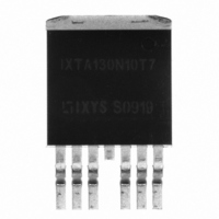
IXTA130N10T7
Manufacturer Part Number
IXTA130N10T7
Description
MOSFET N-CH 100V 130A TO-263-7
Manufacturer
IXYS
Series
TrenchMV™r
Datasheet
1.IXTA130N10T7.pdf
(5 pages)
Specifications of IXTA130N10T7
Fet Type
MOSFET N-Channel, Metal Oxide
Fet Feature
Standard
Rds On (max) @ Id, Vgs
9.1 mOhm @ 25A, 10V
Drain To Source Voltage (vdss)
100V
Current - Continuous Drain (id) @ 25° C
130A
Vgs(th) (max) @ Id
4.5V @ 250µA
Gate Charge (qg) @ Vgs
104nC @ 10V
Input Capacitance (ciss) @ Vds
5080pF @ 25V
Power - Max
360W
Mounting Type
Surface Mount
Package / Case
D²Pak, TO-263 (6 leads + tab)
Configuration
Single
Transistor Polarity
N-Channel
Resistance Drain-source Rds (on)
0.0085 Ohms
Drain-source Breakdown Voltage
100 V
Gate-source Breakdown Voltage
+/- 30 V
Continuous Drain Current
130 A
Power Dissipation
360 W
Maximum Operating Temperature
+ 175 C
Mounting Style
SMD/SMT
Minimum Operating Temperature
- 55 C
Vdss, Max, (v)
100
Id(cont), Tc=25°c, (a)
130
Rds(on), Max, Tj=25°c, (?)
0.0091
Ciss, Typ, (pf)
5080
Qg, Typ, (nc)
104
Trr, Typ, (ns)
67
Trr, Max, (ns)
-
Pd, (w)
360
Rthjc, Max, (k/w)
0.42
Package Style
TO-263 (7-lead)
Lead Free Status / RoHS Status
Lead free / RoHS Compliant


Notes: 1.
IXYS reserves the right to change limits, test conditions, and dimensions.
IXYS MOSFETs and IGBTs are covered
by one or more of the following U.S. patents: 4,850,072
Symbol
(T
g
C
C
C
t
t
t
t
Q
Q
Q
R
Source-Drain Diode
Symbol
(T
I
I
V
t
I
Q
S
SM
RM
d(on)
r
d(off)
f
rr
fs
SD
iss
oss
rss
thJC
g(on)
gs
gd
RM
J
J
= 25°C, unless otherwise specified)
= 25°C, unless otherwise specified)
2. On through-hole packages, R
location must be 5mm or less from the package body
Pulse test, t ≤ 300μs; duty cycle, d ≤ 2%.
Resistive Switching Times
V
R
I
-di/dt = 100A/μs
V
Test Conditions
V
V
V
Test Conditions
V
Repetitive, Pulse width limited by T
I
F
F
GS
R
G
DS
GS
GS
GS
= 25A, V
= 25A, V
= 50V
= 5Ω (External)
= 10V, V
= 0V, V
= 0V
= 10V, I
= 10V, V
GS
GS
DS
D
DS
= 0V
DS
= 0V, Note 1
= 60A, Note 1
= 25V, f = 1MHz
= 20V, I
= 0.5 • V
4,835,592
4,881,106
D
DSS
4,931,844
5,017,508
5,034,796
= 25A
DS(on)
, I
D
= 25
Kelvin test contact
5,049,961
5,063,307
5,187,117
JM
5,237,481
5,381,025
5,486,715
Min.
Min.
Characteristic Values
Characteristic Values
55
6,162,665
6,259,123 B1
6,306,728 B1
5080
Typ.
Typ.
160
635
104
4.7
67
93
95
30
29
44
28
30
47
Max.
Max.
0.42 °C/W
130
350
1.0
6,404,065 B1
6,534,343
6,583,505
nC
nC
nC
pF
pF
pF
nC
ns
ns
ns
ns
ns
S
A
A
V
A
6,683,344
6,710,405 B2 6,759,692
6,710,463
TO-263 (7-lead) (IXTA..7) Outline
6,727,585
6,771,478 B2 7,071,537
IXTA130N10T7
Pins: 1 - Gate
2, 3 - Source
4 - Drain
5,6,7 - Source
Tab (8) - Drain
7,005,734 B2
7,063,975 B2
7,157,338B2
Related parts for IXTA130N10T7
Image
Part Number
Description
Manufacturer
Datasheet
Request
R


Part Number:
Description:
HiPerFET Power MOSFETs
Manufacturer:
IXYS Corporation
Datasheet:
Part Number:
Description:
J-K-Type Flip-Flop
Manufacturer:
IXYS Corporation
Datasheet:
Part Number:
Description:
HiPerRF Power MOSFETs
Manufacturer:
IXYS Corporation
Datasheet:
Part Number:
Description:
Rectifier Module for Three Phase Power Factor Correction
Manufacturer:
IXYS Corporation
Datasheet:
Part Number:
Description:
Thyristor Modules Thyristor/Diode Modules
Manufacturer:
IXYS Corporation
Datasheet:
Part Number:
Description:
Thyristor Modules Thyristor/Diode Modules
Manufacturer:
IXYS Corporation
Datasheet:
Part Number:
Description:
Thyristor Modules Thyristor/Diode Modules
Manufacturer:
IXYS Corporation
Datasheet:
Part Number:
Description:
Thyristor Modules Thyristor/Diode Modules
Manufacturer:
IXYS Corporation
Datasheet:
Part Number:
Description:
Thyristor Modules /Diode Modules
Manufacturer:
IXYS Corporation
Datasheet:
Part Number:
Description:
Thyristor Modules /Diode Modules
Manufacturer:
IXYS Corporation
Datasheet:
Part Number:
Description:
Thyristor Modules Thyristor/Diode Modules
Manufacturer:
IXYS Corporation
Datasheet: