STW43NM50N STMicroelectronics, STW43NM50N Datasheet
STW43NM50N
Specifications of STW43NM50N
Available stocks


Related parts for STW43NM50N


STW43NM50N Summary of contents
Page 1
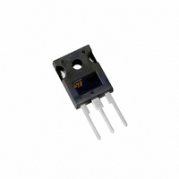
... It is therefore suitable for the most demanding high efficiency converters. Table 1. Device summary Order code STW43NM50N January 2010 R DS(on max < 0.085 Ω Figure 1. Marking 43NM50N Doc ID 14168 Rev 5 STW43NM50N TO-247 TO-247 Internal schematic diagram Package Packaging TO-247 Tube 1/12 www.st.com 12 ...
Page 2
... Contents Contents 1 Electrical ratings . . . . . . . . . . . . . . . . . . . . . . . . . . . . . . . . . . . . . . . . . . . . 3 2 Electrical characteristics . . . . . . . . . . . . . . . . . . . . . . . . . . . . . . . . . . . . . 4 2.1 Electrical characteristics (curves) 3 Test circuits 4 Package mechanical data . . . . . . . . . . . . . . . . . . . . . . . . . . . . . . . . . . . . . 9 5 Revision history . . . . . . . . . . . . . . . . . . . . . . . . . . . . . . . . . . . . . . . . . . . 11 2/ Doc ID 14168 Rev 5 STW43NM50N ...
Page 3
... STW43NM50N 1 Electrical ratings Table 2. Absolute maximum ratings Symbol V Drain-source voltage ( Gate-source voltage GS I Drain current (continuous Drain current (continuous (1) I Drain current (pulsed Total dissipation at T TOT (2) dv/dt Peak diode recovery voltage slope T Storage temperature stg T Max. operating junction temperature j 1. Pulse width limited by safe operating area ≤ ...
Page 4
... Parameter Test conditions V = MHz 400 (see Figure 15) f=1 MHz Gate DC Bias=0 Test signal level = 20 mV open drain DS Doc ID 14168 Rev 5 STW43NM50N Min. Typ 500 250 µ 18.5 A 0.070 0.085 D Min. Typ 4200 - 290 400 V - 590 = 37 A, 140 1.4 oss Max. Unit ...
Page 5
... STW43NM50N Table 7. Switching times Symbol t Turn-on delay time d(on) t Rise time r t Turn-off delay time d(off) t Fall time f Table 8. Source drain diode Symbol I Source-drain current SD (1) I Source-drain current (pulsed) SDM (2) V Forward on voltage SD t Reverse recovery time rr Q Reverse recovery charge ...
Page 6
... Figure 3. AM00875v1 10µs 100µs 1ms 10ms V (V) 100 DS Figure 5. AM00874v1 (V) DS Figure 7. AM00868v1 R DS(on) -50°C 0.74 25°C 150°C 0.72 0.70 0.68 0. Doc ID 14168 Rev 5 STW43NM50N Thermal impedance Transfer characteristics Static drain-source on resistance (Ω) V =10V GS I =18. AM00873v1 V ( AM00870v1 I ...
Page 7
... STW43NM50N Figure 8. Gate charge vs gate-source voltage Figure (V) V =400V =10V GS I =37A 100 Figure 10. Normalized gate threshold voltage vs temperature V GS(th norm 1 1.0 0.9 0.8 0.7 - Figure 12. Source-drain diode forward characteristics V SD (V) 1.0 0.8 0.6 0 AM00872v1 (pF) 10000 1000 100 150 Q (nC) g Figure 11. Normalized on resistance vs ...
Page 8
... Figure 14. Switching times test circuit for resistive load Figure 16. Test circuit for inductive load switching and diode recovery times Figure 18. Unclamped inductive waveform 8/12 Figure 15. Gate charge test circuit Figure 17. Unclamped inductive load test circuit Figure 19. Switching time waveform Doc ID 14168 Rev 5 STW43NM50N ...
Page 9
... STW43NM50N 4 Package mechanical data In order to meet environmental requirements, ST offers these devices in different grades of ECOPACK® packages, depending on their level of environmental compliance. ECOPACK® specifications, grade definitions and product status are available at: www.st.com. ECOPACK® trademark. Doc ID 14168 Rev 5 Package mechanical data ...
Page 10
... L1 L2 øP øR S 10/12 TO-247 Mechanical data mm. Min. Typ 4.85 2.20 1.0 2.0 3.0 0.40 19.85 15.45 5.45 14.20 3.70 18.50 3.55 4.50 5.50 Doc ID 14168 Rev 5 STW43NM50N Max. 5.15 2.60 1.40 2.40 3.40 0.80 20.15 15.75 14.80 4.30 3.65 5.50 ...
Page 11
... STW43NM50N 5 Revision history Table 9. Document revision history Date 15-Nov-2007 04-Aug-2008 15-Oct-2008 27-Jan-2009 08-Jan-2010 Revision 1 First release 2 Document status promoted from preliminary data to datasheet 2.1: Electrical characteristics (curves value has been corrected in GS Table 2: Absolute maximum 5 Updated Doc ID 14168 Rev 5 Revision history ...
Page 12
... Australia - Belgium - Brazil - Canada - China - Czech Republic - Finland - France - Germany - Hong Kong - India - Israel - Italy - Japan - Malaysia - Malta - Morocco - Philippines - Singapore - Spain - Sweden - Switzerland - United Kingdom - United States of America 12/12 Please Read Carefully: © 2010 STMicroelectronics - All rights reserved STMicroelectronics group of companies www.st.com Doc ID 14168 Rev 5 STW43NM50N ...