NJU7112AM-TE1 NJR, NJU7112AM-TE1 Datasheet

Comparator ICs CMOS Comparator w/ Open Drain Output

NJU7112AM-TE1

Manufacturer Part Number
NJU7112AM-TE1
Description
Comparator ICs CMOS Comparator w/ Open Drain Output
Manufacturer
NJR
Datasheet

Specifications of NJU7112AM-TE1

Number Of Channels
2 Channels
Product
Analog Comparators
Output Type
Open Drain
Response Time
2.7 us
Offset Voltage (max)
12 mV
Input Bias Current (max)
1 pA
Supply Voltage (max)
14 V
Supply Voltage (min)
3 V
Supply Current (max)
40 uA
Maximum Power Dissipation
300 mW
Maximum Operating Temperature
+ 70 C
Mounting Style
SMD/SMT
Package / Case
DMP-8
Minimum Operating Temperature
0 C
Lead Free Status / RoHS Status
Lead free / RoHS Compliant
■ GENERAL DESCRIPTION
Comparators performing wide operating voltage from 3 to
16V,low operating current and low offset voltage.
can interface with most of TTL and C-MOS type standard logic
ICs.
■ FEATURES
■ PIN CONFIGURATION
■ EQUIVALENT CIRCUIT
Ver.2003-03-18
● Single-Power-Supply
● Wide Operating Voltage
● Low Operating Current
● Wide Common Mode Input Voltage ( 0~3.8V @ V
● High Input Impedance
● Low Bias Current
● Low Offset Voltage
● Open Drain Output
● Package Outline
● C-MOS Technology
The NJU7112A and 14A dual and quad C-MOS
The NJU7112A and 14A operated on a single-power-supply
C-MOS COMPARATOR WITH OPEN DRAIN OUTPUT
NJU7112AD/AM
( V
( 11µA/circuit typ. )
( I
DIP/DMP8 ( NJU7112A )
DIP/DMP14 ( NJU7114A )
IB
DD
=1pA )
=3~16V )
DD
=5V )
■ PACKAGE OUTLINE
NJU7114AD/AM
NJU7112AD
NJU7114AD
NJU7114AM
NJU7112AM
- 1 -

Related parts for NJU7112AM-TE1

NJU7112AM-TE1 Summary of contents

Page 1

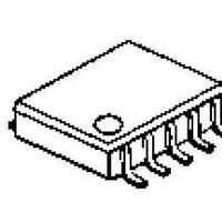
... Low Bias Current ● Low Offset Voltage ● Open Drain Output ● Package Outline ● C-MOS Technology ■ PIN CONFIGURATION NJU7112AD/AM ■ EQUIVALENT CIRCUIT Ver.2003-03-18 ■ PACKAGE OUTLINE ( V =3~16V ) DD ( 11µA/circuit typ =1pA ) IB DIP/DMP8 ( NJU7112A ) DIP/DMP14 ( NJU7114A ) NJU7114AD/AM NJU7112AD NJU7112AM NJU7114AD NJU7114AM - 1 - ...

Page 2

ABSOLUTE MAXIMUM RATINGS PARAMETER Supply Voltage Differential Input Voltage Input Voltage Output Voltage Output Current Power Dissipation Operating Temperature Range Storage Temperature Range ( note1 ) If the supply voltage ( less than 18V, the input ...

Page 3

MEASUREMENT CIRCUIT ■ TIMING WAVEFORM Over Drive Input Output ( L→H ) Ver.2003-03-18 Over Drive Input Output ( H→L ) [CAUTION] The specifications on this databook are only given for information , without any guarantee as regards either mistakes ...

Related keywords