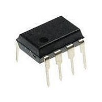
LM311N ON Semiconductor, LM311N Datasheet - Page 3

LM311N
Manufacturer Part Number
LM311N
Description
Comparator ICs 5-30V SGL Comparator
Manufacturer
ON Semiconductor
Datasheet
1.LM311D.pdf
(10 pages)
Specifications of LM311N
Number Of Channels
1 Channel
Output Type
Complementary
Response Time
200 ns
Offset Voltage (max)
7.5 mV
Input Bias Current (max)
100 nA
Supply Voltage (max)
36 V
Supply Voltage (min)
5 V
Supply Current (max)
2.4 mA
Maximum Power Dissipation
625 mW
Maximum Operating Temperature
+ 70 C
Mounting Style
Through Hole
Package / Case
PDIP-8
Minimum Operating Temperature
0 C
Lead Free Status / RoHS Status
Lead free / RoHS Compliant
Available stocks
Company
Part Number
Manufacturer
Quantity
Price
Part Number:
LM311N
Manufacturer:
FAIRCHILD/仙童
Quantity:
20 000
Part Number:
LM311N/NOPB
Manufacturer:
TI/德州仪器
Quantity:
20 000
Company:
Part Number:
LM311NG
Manufacturer:
ON Semiconductor
Quantity:
3 650
Part Number:
LM311NG
Manufacturer:
ON/安森美
Quantity:
20 000
* LM211: T
1. Offset voltage, offset current and bias current specifications apply for a supply voltage range from a single 5.0 V supply up to ±15 V supplies.
2. This rating applies for ±15 V supplies. The positive input voltage limit is 30 V above the negative supply. The negative input voltage limit is
3. The offset voltages and offset currents given are the maximum values required to drive the output within a volt of either supply with a 1.0 mA
4. The response time specified is for a 100 mV input step with 5.0 mV overdrive.
5. Do not short the strobe pin to ground; it should be current driven at 3.0 mA to 5.0 mA.
ELECTRICAL CHARACTERISTICS
LM311: T
Input Offset Voltage (Note 3)
Input Offset Current (Note 3) T
Input Bias Current T
Voltage Gain
Response Time (Note 4)
Saturation Voltage
Strobe ”On” Current (Note 5)
Output Leakage Current
Input Voltage Range (T
Positive Supply Current
Negative Supply Current
equal to the negative supply voltage or 30 V below the positive supply, whichever is less.
load. Thus, these parameters define an error band and take into account the “worst case” effects of voltage gain and input impedance.
R
R
T
T
V
V
V
V
Balance/Strobe
low
low
CC
ID
ID ≥ 10 mV,
ID ≥ 5.0 mV,
S
S
V
V
V
V
≤ 50 kW, T
≤ 50 kW, T
ID
ID
ID
ID
≥ 5.0 mV, V
≤ T
≤ T
≥ 4.5 V, V
≤ −5.0 mV, I
≤−10 mV, I
6≤6.0 mV, I
6≤10 mV, I
low
low
Balance
A
A
≤ T
≤ T
= −25°C, T
= 0°C, T
Inputs
V
V
high
high
O
O
3
A
low
= 35 V, T
EE
5
6
2
= 35 V, T
O
= +25°C
*
*
= 35 V, T
Characteristic
O
sink
≤ T
= 0, T
A
sink
high
O
= 50 mA, T
300
= +25°C
300
1.3 k
= 50 mA, T
high
A
low
≤ 8.0 mA
≤ 8.0 mA
= +70°C
≤ T
A
low
low
≤ T
= +85°C
= 25°C, I
A
high
≤ T
= 25°C, I
≤ T
A
A
*
≤ T
A
1.3 k
= +25°C
A
A
A
= 25°C
≤ T
≤ T
high
= 25°C
strobe
high
high
strobe
*)
3.7 k
*
(V
= 3.0 mA
*
= 3.0 mA
CC
100
= +15 V, V
3.7 k
800
730
Figure 2. Circuit Schematic
http://onsemi.com
LM211, LM311
340
EE
800
Symbol
= −15 V, T
V
V
V
I
I
I
A
I
I
CC
ICR
EE
IO
IB
OL
S
IO
V
3
A
250
= 25°C, unless otherwise noted) Note 1
3.0 k
−14.5
1.3 k
1.3 k
Min
40
−
−
−
−
−
−
−
−
−
−
−
−
−
−
−
−
−
LM211
900
800
5.4 k
−14.7
0.75
0.23
13.8
+2.4
−1.3
Typ
200
200
0.7
1.7
3.0
0.2
0.1
45
to
−
−
−
−
−
−
300
+13.0
Max
+6.0
−5.0
100
150
3.0
4.0
1.5
0.4
0.5
10
20
10
−
−
−
−
−
−
−14.5
Min
40
−
−
−
−
−
−
−
−
−
−
−
−
−
−
−
−
−
LM311
5.0 k
−14.7
0.75
0.23
13.8
+2.4
−1.3
Typ
200
200
2.0
1.7
3.0
0.2
45
to
−
−
−
−
−
−
−
600
+13.0
Max
+7.5
−5.0
250
300
7.5
1.5
0.4
200
10
50
70
50
−
−
−
−
−
−
−
4
8
1
7
V
Output
GND
V
CC
EE
V/mV
Unit
mV
mA
mA
mA
nA
nA
nA
nA
mA
ns
V
V


