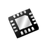
MCP4232T-104-E/ML Microchip Technology, MCP4232T-104-E/ML Datasheet - Page 53

MCP4232T-104-E/ML
Manufacturer Part Number
MCP4232T-104-E/ML
Description
Digital Potentiometer ICs Dual 7B V SPI Rheo
Manufacturer
Microchip Technology
Datasheet
1.MCP4151-502EMF.pdf
(82 pages)
Specifications of MCP4232T-104-E/ML
Number Of Pots
Dual
Taps Per Pot
128
Resistance
100 KOhms
Wiper Memory
Volatile
Digital Interface
Serial (SPI)
Operating Supply Voltage
2.5 V, 3.3 V, 5 V
Supply Current
1 mA
Maximum Operating Temperature
+ 125 C
Minimum Operating Temperature
- 40 C
Mounting Style
SMD/SMT
Supply Voltage (max)
5.5 V
Supply Voltage (min)
1.8 V
Package / Case
QFN EP-16
Lead Free Status / RoHS Status
Lead free / RoHS Compliant
7.6
The Read command is a 16-bit command. The format
of the command is shown in
The first 6-bits of the Read command determine the
address and the command. The 7th clock will output
the CMDERR bit on the SDO pin. The remaining
9-clocks the device will transmit the 9 data bits (D8:D0)
of the specified address (AD3:AD0).
Figure 7-4
Read command.
FIGURE 7-4:
© 2007 Microchip Technology Inc.
SDI
SDO
Note:
A
D
3
1
1
Read Data
Normal and High Voltage
shows the SDI and SDO information for a
The High Voltage Read Data command is
supported for compatability with system
that also support MCP414X/416X/424X/
426X devices.
D
A
2
1
1
COMMAND BYTE
D
A
1
1
1
D
A
0
1
1
Read Command - SDI and SDO States.
1
1
1
Figure
1
1
1
X
1
0
7-4.
D
X
8
0
D
X
7
0
D
X
6
0
READ DATA
X
D
5
0
MCP413X/415X/423X/425X
DATA BYTE
X
D
4
0
X
D
3
0
X
D
2
0
7.6.1
The read operation requires that the CS pin be in the
active state (V
the inactive state (V
(V
Byte and Data Byte) is then clocked in on the SCK and
SDI pins. The SDO pin starts driving data on the 7th bit
(CMDERR bit) and the addressed data comes out on
the 8th through 16th clocks.
Figure 6-6
Figure 6-5
forms when the SDI and SDO signals are multiplexed
on the same pin. For additional information on the mul-
tiplexing of these signals, refer to Section 6.1.3 “SDI/
SDO”.
D
X
1
0
IL
or V
D
X
0
0 Attempted Memory Read of Reserved
IHH
Valid Address/Command combination
Memory location.
show possible waveforms for a single read.
and
). The 16-bit Read Command (Command
SINGLE READ
IL
Figure 6-6
or V
IHH
IH
) and is driven to the active state
). Typically, the CS pin will be in
show the single read wave-
Figure 6-3
DS22060A-page 53
through


