FDD6N20TM Fairchild Semiconductor, FDD6N20TM Datasheet

MOSFET N-CH 200V 4.5A DPAK

FDD6N20TM

Manufacturer Part Number
FDD6N20TM
Description
MOSFET N-CH 200V 4.5A DPAK
Manufacturer
Fairchild Semiconductor
Series
UniFET™r
Datasheet

Specifications of FDD6N20TM

Fet Type
MOSFET N-Channel, Metal Oxide
Fet Feature
Standard
Rds On (max) @ Id, Vgs
800 mOhm @ 2.3A, 10V
Drain To Source Voltage (vdss)
200V
Current - Continuous Drain (id) @ 25° C
4.5A
Vgs(th) (max) @ Id
5V @ 250µA
Gate Charge (qg) @ Vgs
6.1nC @ 10V
Input Capacitance (ciss) @ Vds
230pF @ 25V
Power - Max
40W
Mounting Type
Surface Mount
Package / Case
DPak, TO-252 (2 leads+tab), SC-63
Configuration
Single
Transistor Polarity
N-Channel
Resistance Drain-source Rds (on)
0.8 Ohms
Drain-source Breakdown Voltage
200 V
Gate-source Breakdown Voltage
+/- 30 V
Continuous Drain Current
4.5 A
Power Dissipation
40 W
Maximum Operating Temperature
+ 150 C
Mounting Style
SMD/SMT
Fall Time
12.8 ns
Minimum Operating Temperature
- 55 C
Rise Time
5.6 ns
Lead Free Status / RoHS Status
Lead free / RoHS Compliant
Other names
FDD6N20TM

Available stocks

Company
Part Number
Manufacturer
Quantity
Price
Company:
Part Number:
FDD6N20TM
Quantity:
2 500
©2007 Fairchild Semiconductor Corporation
FDD6N20 / FDU6N20 Rev. A
MOSFET Maximum Ratings
*Drain current limited by maximum junction temperature
Thermal Characteristics
V
V
I
I
E
I
E
dv/dt
P
T
T
R
R
D
DM
AR
FDD6N20 / FDU6N20
N-Channel MOSFET
200V, 4.5A, 0.8Ω
Features
• R
• Low gate charge ( Typ. 4.7nC )
• Low C
• Fast switching
• 100% avalanche tested
• Improved dv/dt capability
• RoHS compliant
J
L
DSS
GSS
AS
AR
D
θJC
θJA
, T
Symbol
Symbol
STG
DS(on)
rss
= 0.6Ω ( Typ. )@ V
( Typ. 6.3pF )
Drain to Source Voltage
Gate to Source Voltage
Drain Current
Drain Current
Single Pulsed Avalanche Energy
Avalanche Current
Repetitive Avalanche Energy
Peak Diode Recovery dv/dt
Power Dissipation
Operating and Storage Temperature Range
Maximum Lead Temperature for Soldering Purpose,
1/8” from Case for 5 Seconds
Thermal Resistance, Junction to Case
Thermal Resistance, Junction to Ambient
G
S
FDD Series
D-PAK
GS
= 10V, I
D
D
= 2.3A
T
C
= 25
Parameter
Parameter
-Continuous (T
-Continuous (T
(T
- Derate above 25
- Pulsed
C
o
C unless otherwise noted*
= 25
G
D S
o
C)
C
C
FDU Series
= 25
= 100
I-PAK
1
o
C
o
Description
These N-Channel enhancement mode power field effect
transistors are produced using Fairchild’s proprietary, planar
stripe, DMOS technology.
This advanced technology has been especially tailored to
minimize on-state resistance, provide superior
performance, and withstand high energy pulse in the avalanche
and commutation mode. These devices are well suited for high
efficient switched mode power supplies and active power factor
correction.
C)
o
C)
(Note 1)
(Note 2)
(Note 1)
(Note 1)
(Note 3)
G
-55 to +150
Ratings
Ratings
0.32
200
±30
300
4.5
2.7
4.5
4.0
4.5
110
S
18
60
40
3.1
D
UniFET
www.fairchildsemi.com
May 2007
switching
Units
W/
Units
o
V/ns
mJ
mJ
C/W
o
o
W
V
V
A
A
A
C
C
o
C
TM
tm

Related parts for FDD6N20TM

FDD6N20TM Summary of contents

Page 1

... Thermal Characteristics Symbol R Thermal Resistance, Junction to Case θJC R Thermal Resistance, Junction to Ambient θJA ©2007 Fairchild Semiconductor Corporation FDD6N20 / FDU6N20 Rev. A Description = 2.3A These N-Channel enhancement mode power field effect D transistors are produced using Fairchild’s proprietary, planar stripe, DMOS technology. This advanced technology has been especially tailored to ...

Page 2

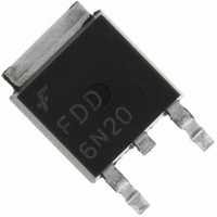
... Package Marking and Ordering Information Device Marking Device FDD6N20 FDD6N20TM FDD6N20 FDD6N20TF FDU6N20 FDU6N20TU Electrical Characteristics Symbol Parameter Off Characteristics BV Drain to Source Breakdown Voltage DSS ΔBV Breakdown Voltage Temperature DSS ΔT / Coefficient J I Zero Gate Voltage Drain Current DSS I Gate to Body Leakage Current ...

Page 3

Typical Performance Characteristics Figure 1. On-Region Characteristics 15 10 8.0 V 7.0 V 6.5 V 6 *Notes: 0.1 0 ,Drain-Source Voltage[V] DS Figure 3. On-Resistance Variation vs. ...

Page 4

Typical Performance Characteristics Figure 7. Breakdown Voltage Variation vs. Temperature 1.2 1.1 1.0 0.9 0.8 -100 - Junction Temperature J Figure 9. Maximum Safe Operating Area Operation in This Area is Limited by ...

Page 5

FDD6N20 / FDU6N20 Rev. A Gate Charge Test Circuit & Waveform Resistive Switching Test Circuit & Waveforms Unclamped Inductive Switching Test Circuit & Waveforms 5 www.fairchildsemi.com ...

Page 6

...

Page 7

Mechanical Dimensions FDD6N20 / FDU6N20 Rev. A D-PAK 7 www.fairchildsemi.com ...

Page 8

Mechanical Dimensions FDD6N20 / FDU6N20 Rev. A I-PAK 8 www.fairchildsemi.com ...

Page 9

... TRADEMARKS The following are registered and unregistered trademarks and service marks Fairchild Semiconductor owns or is authorized to use and is not intended exhaustive list of all such trademarks. ® ACEx Green FPS™ e-Series™ Build it Now™ GOT™ CorePLUS™ i-Lo™ ...

Related keywords