SIE806DF-T1-E3 Vishay, SIE806DF-T1-E3 Datasheet

MOSFET N-CH 30V 60A 10-POLARPAK

SIE806DF-T1-E3

Manufacturer Part Number
SIE806DF-T1-E3
Description
MOSFET N-CH 30V 60A 10-POLARPAK
Manufacturer
Vishay
Series
TrenchFET®r
Datasheets

Specifications of SIE806DF-T1-E3

Fet Type
MOSFET N-Channel, Metal Oxide
Fet Feature
Standard
Rds On (max) @ Id, Vgs
1.7 mOhm @ 25A, 10V
Drain To Source Voltage (vdss)
30V
Current - Continuous Drain (id) @ 25° C
60A
Vgs(th) (max) @ Id
2V @ 250µA
Gate Charge (qg) @ Vgs
250nC @ 10V
Input Capacitance (ciss) @ Vds
13000pF @ 15V
Power - Max
125W
Mounting Type
Surface Mount
Package / Case
10-PolarPAK® (L)
Transistor Polarity
N Channel
Continuous Drain Current Id
60A
Drain Source Voltage Vds
30V
On Resistance Rds(on)
2.1mohm
Rds(on) Test Voltage Vgs
12V
Threshold Voltage Vgs Typ
1.3V
Configuration
Single Quad Drain Dual Gate Quad Source
Resistance Drain-source Rds (on)
0.0017 Ohms
Drain-source Breakdown Voltage
30 V
Gate-source Breakdown Voltage
+/- 12 V
Continuous Drain Current
41.3 A
Power Dissipation
5.2 W
Maximum Operating Temperature
+ 150 C
Mounting Style
SMD/SMT
Minimum Operating Temperature
- 50 C
Lead Free Status / RoHS Status
Lead free / RoHS Compliant
Lead Free Status / RoHS Status
Lead free / RoHS Compliant, Lead free / RoHS Compliant
Other names
SIE806DF-T1-E3TR
Document Number: 73740
S09-1337-Rev. B, 13-Jul-09
Notes:
a. Package limited is 60 A.
b. Surface Mounted on 1" x 1" FR4 board.
c. t = 10 s.
d. See Solder Profile (www.vishay.com/doc?73257). The PolarPAK is a leadless package. The end of the lead terminal is exposed copper not
e. Rework Conditions: manual soldering with a soldering iron is not recommended for leadless components.
Package Drawing
www.vishay.com/doc?72945
Ordering Information:
Top surface is connected to pins 1, 5, 6, and 10
V
PRODUCT SUMMARY
ABSOLUTE MAXIMUM RATINGS T
Parameter
Drain-Source Voltage
Gate-Source Voltage
Continuous Drain Current (T
Pulsed Drain Current
Continuous Source-Drain Diode Current
Single Pulse Avalanche Current
Avalanche Energy
Maximum Power Dissipation
Operating Junction and Storage Temperature Range
Soldering Recommendations (Peak Temperature)
DS
required to ensure adequate bottom side solder interconnection.
plated) as a result of the singulation process in manufacturing. A solder fillet at the exposed copper tip cannot be guaranteed and is not
30
(V)
10
D
D
1
G
0.0021 at V
2
G
0.0017 at V
9
Top View
S
3
S
8
R
D
DS(on)
SiE806DF -T1-E3
SiE806DF-T1-GE3 (Lead (Pb)-free and Halogen-free)
S
4
S
GS
7
GS
(Ω)
= 4.5 V
= 10 V
e
D
5
D
6
J
PolarPAK
= 150 °C)
Silicon
(Lead (Pb)-free)
Limit
202
187
N-Channel 30-V (D-S) MOSFET
6
D
5
I
D
(A)
7
Bottom View
4
Package
Limit
S
60
60
d, e
L = 0.1 mH
T
T
T
T
T
T
T
T
T
T
8
C
C
C
C
C
A
A
A
A
A
A
3
= 25 °C
= 70 °C
= 25 °C
= 25 °C
= 70 °C
= 25 °C
= 70 °C
= 25 °C
= 25 °C
= 70 °C
= 25 °C, unless otherwise noted
G
Q
9
2
g
75 nC
(Typ.)
10
D
1
Symbol
T
J
V
V
E
I
I
P
, T
DM
I
I
AS
DS
GS
AS
D
S
D
FEATURES
APPLICATIONS
stg
• Halogen-free According to IEC 61249-2-21
• TrenchFET
• Ultra Low Thermal Resistance Using Top-
• Leadframe-Based New Encapsulated Package
• Low Q
• 100 % R
• Compliant to RoHS directive 2002/95/EC
• VRM
• DC/DC Conversion: Low-Side
• Synchronous Rectification
Definition
Exposed PolarPAK
Cooling
- Die Not Exposed
- Same Layout Regardless of Die Size
gd
/Q
g
and UIS Tested
gs
®
Gen II Power MOSFET
Ratio Helps Prevent Shoot-Through
60
202 (Silicon Limit)
a
(Package Limit)
- 55 to 150
®
41.3
4.3
5.2
3.3
Limit
33
Package for Double-Sided
± 12
100
125
125
60
60
260
30
50
80
b, c
b, c
b, c
b, c
a
b, c
a
Vishay Siliconix
G
www.vishay.com/ppg?73740
For Related Documents
N-Channel MOSFET
SiE806DF
www.vishay.com
D
S
Unit
mJ
°C
W
V
A
1

Related parts for SIE806DF-T1-E3

SIE806DF-T1-E3 Summary of contents

Page 1

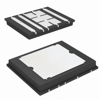
... Top View Top surface is connected to pins and 10 Ordering Information: SiE806DF -T1-E3 (Lead (Pb)-free) SiE806DF-T1-GE3 (Lead (Pb)-free and Halogen-free) ABSOLUTE MAXIMUM RATINGS T Parameter Drain-Source Voltage Gate-Source Voltage Continuous Drain Current (T = 150 °C) J Pulsed Drain Current Continuous Source-Drain Diode Current Single Pulse Avalanche Current ...

Page 2

... SiE806DF Vishay Siliconix THERMAL RESISTANCE RATINGS Parameter a, b Maximum Junction-to-Ambient Maximum Junction-to-Case (Drain Top Maximum Junction-to-Case (Source) Notes: a. Surface Mounted on 1" x 1" FR4 board. b. Maximum under Steady State conditions is 68 °C/W. c. Measured at source pin (on the side of the package). SPECIFICATIONS °C, unless otherwise noted ...

Page 3

... On-Resistance vs. Drain Current and Gate Voltage Total Gate Charge (nC) g Gate Charge Document Number: 73740 S09-1337-Rev. B, 13-Jul- thru 0.3 0.4 0 100 120 150 180 SiE806DF Vishay Siliconix 125 ° ° ° 1.0 1.5 2 Gate-to-Source Voltage (V) GS Transfer Characteristics 15 000 C iss 12 000 9000 6000 3000 C oss C rss ...

Page 4

... SiE806DF Vishay Siliconix TYPICAL CHARACTERISTICS 25 °C, unless otherwise noted 100 T = 150 ° 0.0 0.2 0.4 0 Source-to-Drain Voltage (V) SD Source-Drain Diode Forward Voltage 1.8 1 250 µA D 1.4 1.2 1.0 0.8 0 Temperature (°C) J Threshold Voltage Limited by R www.vishay.com 4 0.0050 0.0045 0.0040 0.0035 ° ...

Page 5

... It is used to determine the current rating, when this rating falls below the package limit. Document Number: 73740 S09-1337-Rev. B, 13-Jul-09 140 120 100 100 125 150 = 150 °C, using junction-to-case thermal resistance, and is more useful in settling the upper J(max) SiE806DF Vishay Siliconix 100 125 T - Case Temperature (° ...

Page 6

... SiE806DF Vishay Siliconix TYPICAL CHARACTERISTICS 25 °C, unless otherwise noted 2 1 Duty Cycle = 0.5 0.2 0.1 0.1 0.05 0.02 0. Duty Cycle = 0.5 0.2 0.1 0.05 0.1 0.02 Single Pulse 0. Normalized Thermal Transient Impedance, Junction-to-Case (Drain Top Duty Cycle = 0.5 0.2 0.1 0.1 ...

Page 7

... Vishay product could result in personal injury or death. Customers using or selling Vishay products not expressly indicated for use in such applications their own risk and agree to fully indemnify and hold Vishay and its distributors harmless from and against any and all claims, liabilities, expenses and damages arising or resulting in connection with such use or sale, including attorneys fees, even if such claim alleges that Vishay or its distributor was negligent regarding the design or manufacture of the part ...

Related keywords