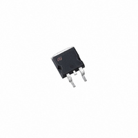
STB180N55F3 STMicroelectronics, STB180N55F3 Datasheet - Page 5

STB180N55F3
Manufacturer Part Number
STB180N55F3
Description
MOSFET N-CH 55V 120A D2PAK
Manufacturer
STMicroelectronics
Series
STripFET™r
Datasheet
1.STB180N55F3.pdf
(14 pages)
Specifications of STB180N55F3
Fet Type
MOSFET N-Channel, Metal Oxide
Fet Feature
Standard
Rds On (max) @ Id, Vgs
3.5 mOhm @ 60A, 10V
Drain To Source Voltage (vdss)
55V
Current - Continuous Drain (id) @ 25° C
120A
Vgs(th) (max) @ Id
4V @ 250µA
Gate Charge (qg) @ Vgs
100nC @ 10V
Input Capacitance (ciss) @ Vds
6800pF @ 25V
Power - Max
330W
Mounting Type
Surface Mount
Package / Case
D²Pak, TO-263 (2 leads + tab)
Configuration
Single
Transistor Polarity
N-Channel
Resistance Drain-source Rds (on)
0.0035 Ohms
Drain-source Breakdown Voltage
55 V
Gate-source Breakdown Voltage
+/- 20 V
Continuous Drain Current
120 A
Power Dissipation
330 W
Maximum Operating Temperature
+ 175 C
Mounting Style
SMD/SMT
Minimum Operating Temperature
- 55 C
Lead Free Status / RoHS Status
Lead free / RoHS Compliant
Other names
497-7939-2
STB180N55F3
STB180N55F3
Available stocks
Company
Part Number
Manufacturer
Quantity
Price
Company:
Part Number:
STB180N55F3
Manufacturer:
ST
Quantity:
12 500
Part Number:
STB180N55F3
Manufacturer:
ST
Quantity:
20 000
STB180N55F3 - STP180N55F3
Table 5.
1. Pulse width limited by safe operating area
2. Pulsed: pulse duration = 300µs, duty cycle 1.5%
Symbol
I
V
SDM
I
RRM
SD
I
Q
SD
t
rr
rr
(2)
(1)
Source drain diode
Source-drain current
Source-drain current
(pulsed)
Forward on voltage
Reverse recovery time
Reverse recovery charge
Reverse recovery current
Parameter
I
I
di/dt = 100A/µs,
V
(see
SD
SD
DD
=120A, V
=120A,
Test conditions
=35V, Tj=150°C
Figure
14)
GS
=0
Min.
Electrical characteristics
Typ.
0.11
3.5
60
Max.
120
480
1.5
Unit
µC
ns
A
A
V
A
5/14


