IRFBE30SPBF Vishay, IRFBE30SPBF Datasheet - Page 2
IRFBE30SPBF
Manufacturer Part Number
IRFBE30SPBF
Description
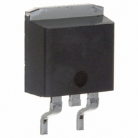
MOSFET N-CH 800V 4.1A D2PAK
Manufacturer
Vishay
Specifications of IRFBE30SPBF
Transistor Polarity
N-Channel
Fet Type
MOSFET N-Channel, Metal Oxide
Fet Feature
Standard
Rds On (max) @ Id, Vgs
3 Ohm @ 2.5A, 10V
Drain To Source Voltage (vdss)
800V
Current - Continuous Drain (id) @ 25° C
4.1A
Vgs(th) (max) @ Id
4V @ 250µA
Gate Charge (qg) @ Vgs
78nC @ 10V
Input Capacitance (ciss) @ Vds
1300pF @ 25V
Power - Max
125W
Mounting Type
Surface Mount
Package / Case
D²Pak, TO-263 (2 leads + tab)
Minimum Operating Temperature
- 55 C
Configuration
Single
Resistance Drain-source Rds (on)
3 Ohm @ 10 V
Drain-source Breakdown Voltage
800 V
Gate-source Breakdown Voltage
+/- 20 V
Continuous Drain Current
4.1 A
Power Dissipation
125000 mW
Maximum Operating Temperature
+ 150 C
Mounting Style
SMD/SMT
Continuous Drain Current Id
4.1A
Drain Source Voltage Vds
800V
On Resistance Rds(on)
3ohm
Rds(on) Test Voltage Vgs
10V
Threshold Voltage Vgs Typ
4V
Lead Free Status / RoHS Status
Lead free / RoHS Compliant
Lead Free Status / RoHS Status
Lead free / RoHS Compliant, Lead free / RoHS Compliant
Other names
*IRFBE30SPBF
Available stocks
Company
Part Number
Manufacturer
Quantity
Price


Document Number: 91119
Notes:
‚
ƒ
„
V
∆ΒV
R
V
gfs
I
I
Q
Q
Q
t
t
t
t
L
L
C
C
C
I
I
V
t
Q
t
Static @ T
Diode Characteristics
DSS
GSS
d(on)
r
d(off)
f
S
SM
rr
on
D
S
(BR)DSS
DS(on)
GS(th)
iss
oss
rss
SD
g
gs
gd
rr
Repetitive rating; pulse width limited by
I
I
Pulse width ≤ 300µs; duty cycle ≤ 2%.
max. junction temperature. (See fig. 11).
T
V
SD
AS
J
DSS
DD
≤ 150°C.
≤ 4.1A, di/dt ≤ 100A/µs, V
= 4.1A. (See Figure 12).
=50V, starting T
/∆T
J
J
Drain-to-Source Breakdown Voltage
Breakdown Voltage Temp. Coefficient
Static Drain-to-Source On-Resistance
Gate Threshold Voltage
Forward Transconductance
Drain-to-Source Leakage Current
Gate-to-Source Forward Leakage
Gate-to-Source Reverse Leakage
Total Gate Charge
Gate-to-Source Charge
Gate-to-Drain ("Miller") Charge
Turn-On Delay Time
Rise Time
Turn-Off Delay Time
Fall Time
Internal Drain Inductance
Internal Source Inductance
Input Capacitance
Output Capacitance
Reverse Transfer Capacitance
Continuous Source Current
(Body Diode)
Pulsed Source Current
(Body Diode)
Diode Forward Voltage
Reverse Recovery Time
Reverse Recovery Charge
Forward Turn-On Time
= 25°C (unless otherwise specified)
Parameter
J
= 25°C, L=29mH, R
Parameter
™
DD
≤ 600,
G
=25Ω
,
Intrinsic turn-on time is negligible (turn-on is dominated by LS+LD)
Min. Typ. Max. Units
Min. Typ. Max. Units
800
–––
–––
–––
–––
–––
–––
–––
–––
–––
–––
–––
–––
–––
–––
–––
–––
–––
–––
–––
–––
–––
–––
–––
2.0
2.5
1300
0.90
–––
–––
–––
–––
–––
–––
–––
–––
–––
–––
–––
310
190
–––
–––
–––
480
4.5
7.5
1.8
12
33
82
30
-100
–––
–––
–––
100
500
100
–––
–––
–––
–––
–––
–––
–––
–––
–––
720
3.0
4.0
9.6
4.1
1.8
2.7
78
45
16
V/°C
nC
nH
nC
µA
nA
pF
ns
ns
Ω
V
V
S
A
V
V
Reference to 25°C, I
V
V
V
V
V
V
V
I
V
V
V
I
R
R
Between lead,
6mm (0.25in.)
from package
and center of die contact
V
V
ƒ = 1.0MHz, See Fig. 5
MOSFET symbol
showing the
integral reverse
p-n junction diode.
T
T
di/dt = 100A/µs
D
D
J
J
GS
GS
DS
DS
DS
DS
GS
GS
DS
GS
DD
G
D
GS
DS
= 4.1A
= 4.1A
= 25°C, I
= 25°C, I
= 12Ω
= 95Ω, See Fig. 10
= 0V, I
= 10V, I
= V
= 100V, I
= 800V, V
= 640V, V
= 20V
= -20V
= 400V
= 10V, See Fig. 6 & 13
= 400V
= 0V
= 25V
GS
, I
D
Conditions
Conditions
D
S
F
D
= 250µA
D
= 250µA
= 4.1A
= 4.1A, V
= 2.5A
GS
GS
= 2.5A
f
= 0V
= 0V, T
www.vishay.com
D
f
= 1mA
f
GS
G
J
= 125°C
G
= 0V
f
f
S
D
D
S
2
Related parts for IRFBE30SPBF
Image
Part Number
Description
Manufacturer
Datasheet
Request
R

Part Number:
Description:
MOSFET N-CH 800V 4.1A TO-220AB
Manufacturer:
Vishay
Datasheet:

Part Number:
Description:
357-036-542-201 CARDEDGE 36POS DL .156 BLK LOPRO
Manufacturer:
Vishay
Datasheet:
Part Number:
Description:
357-036-542-201 CARDEDGE 36POS DL .156 BLK LOPRO
Manufacturer:
Vishay
Datasheet:
Part Number:
Description:
357-036-542-201 CARDEDGE 36POS DL .156 BLK LOPRO
Manufacturer:
Vishay
Datasheet:
Part Number:
Description:
357-036-542-201 CARDEDGE 36POS DL .156 BLK LOPRO
Manufacturer:
Vishay
Datasheet:
Part Number:
Description:
357-036-542-201 CARDEDGE 36POS DL .156 BLK LOPRO
Manufacturer:
Vishay
Datasheet:
Part Number:
Description:
357-036-542-201 CARDEDGE 36POS DL .156 BLK LOPRO
Manufacturer:
Vishay
Datasheet:
Part Number:
Description:
357-036-542-201 CARDEDGE 36POS DL .156 BLK LOPRO
Manufacturer:
Vishay
Datasheet:
Part Number:
Description:
357-036-542-201 CARDEDGE 36POS DL .156 BLK LOPRO
Manufacturer:
Vishay
Datasheet:
Part Number:
Description:
357-036-542-201 CARDEDGE 36POS DL .156 BLK LOPRO
Manufacturer:
Vishay
Datasheet:
Part Number:
Description:
357-036-542-201 CARDEDGE 36POS DL .156 BLK LOPRO
Manufacturer:
Vishay
Datasheet:
Part Number:
Description:
357-036-542-201 CARDEDGE 36POS DL .156 BLK LOPRO
Manufacturer:
Vishay
Datasheet:
Part Number:
Description:
357-036-542-201 CARDEDGE 36POS DL .156 BLK LOPRO
Manufacturer:
Vishay
Datasheet:
Part Number:
Description:
357-036-542-201 CARDEDGE 36POS DL .156 BLK LOPRO
Manufacturer:
Vishay
Datasheet:
Part Number:
Description:
357-036-542-201 CARDEDGE 36POS DL .156 BLK LOPRO
Manufacturer:
Vishay
Datasheet: