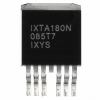
IXTA180N085T7 IXYS, IXTA180N085T7 Datasheet
首页 Discrete Semiconductor Products MOSFETs, GaNFETs - Single IXTA180N085T7
Manufacturer Part Number
IXTA180N085T7
Description
MOSFET N-CH 85V 180A TO-263-7
Specifications of IXTA180N085T7
Fet Type
MOSFET N-Channel, Metal Oxide
Fet Feature
Standard
Rds On (max) @ Id, Vgs
5.5 mOhm @ 25A, 10V
Drain To Source Voltage (vdss)
85V
Current - Continuous Drain (id) @ 25° C
180A
Vgs(th) (max) @ Id
4V @ 250µA
Gate Charge (qg) @ Vgs
170nC @ 10V
Input Capacitance (ciss) @ Vds
7500pF @ 25V
Power - Max
430W
Mounting Type
Surface Mount
Package / Case
D²Pak, TO-263 (6 leads + tab)
Configuration
Single Quint Source
Transistor Polarity
N-Channel
Resistance Drain-source Rds (on)
0.0055 Ohms
Drain-source Breakdown Voltage
85 V
Continuous Drain Current
180 A
Power Dissipation
430 W
Maximum Operating Temperature
+ 175 C
Mounting Style
SMD/SMT
Minimum Operating Temperature
- 55 C
Vdss, Max, (v)
85
Id(cont), Tc=25°c, (a)
180
Rds(on), Max, Tj=25°c, (?)
0.0055
Ciss, Typ, (pf)
8800
Qg, Typ, (nc)
170
Trr, Typ, (ns)
63
Trr, Max, (ns)
-
Pd, (w)
430
Rthjc, Max, (k/w)
0.35
Package Style
TO-263 (7-Lead)
Lead Free Status / RoHS Status
Lead free / RoHS Compliant
TrenchMV
Power MOSFET
N-Channel Enhancement Mode
Avalanche Rated
Symbol
V
V
V
I
I
I
I
E
dv/dt
P
T
T
T
T
T
Weight
Symbol
(T
BV
V
I
I
R
© 2006 IXYS CORPORATION All rights reserved
D25
LRMS
DM
AR
GSS
DSS
L
SOLD
DGR
D
J
JM
stg
GS(th)
DSS
GSM
AS
DS(on)
J
DSS
= 25° C unless otherwise specified)
Test Conditions
T
T
Transient
T
Package Current Limit, RMS
T
T
T
I
T
T
1.6 mm (0.062 in.) from case for 10 s
Plastic body for 10 seconds
Test Conditions
V
V
V
V
V
V
S
C
C
C
C
C
GS
J
J
J
DS
GS
DS
GS
GS
= 25° C to 175° C
= 25° C to 175° C; R
= 25° C
= 25° C, pulse width limited by T
= 25° C
= 25° C
≤ I
≤ 175° C, R
= 25° C
= 0 V, I
= V
= ± 20 V, V
= V
= 0 V
= 10 V, I
DM
, di/dt ≤ 100 A/µs, V
GS
TM
DSS
, I
D
D
= 250 µA
D
= 250 µA
G
= 25 A, Note 1
DS
= 5 Ω
= 0 V
Preliminary Technical Information
GS
= 1 MΩ
DD
IXTA180N085T7
T
J
≤ V
= 150° C
DSS
JM
Min.
2.0
85
Characteristic Values
-55 ... +175
-55 ... +175
Maximum Ratings
Typ.
4.2
± 20
180
160
480
430
300
260
175
1.0
85
85
25
± 200
3
3
250
Max.
4.0
5.5
5
V/ns
m Ω
nA
µA
µA
°C
°C
°C
°C
°C
W
V
V
V
A
A
A
V
A
g
V
J
TO-263 (7-lead) (IXTA..7)
Features
Advantages
Applications
Pin-out:1 - Gate
Ultra-low On Resistance
Unclamped Inductive Switching (UIS)
rated
Low package inductance
- easy to drive and to protect
175 ° C Operating Temperature
Easy to mount
Space savings
High power density
- Motor Drives
- 42V Power Bus
- ABS Systems
Primary Switch for 24V and 48V
V
I
R
DC/DC Converters and Off-line UPS
High Current Switching
D25
Systems
Applications
Automotive
DSS
DS(on)
1
2, 3 - Source
4 - NC (cut)
5,6,7 - Source
TAB (8) - Drain
7
=
= 180
≤ ≤ ≤ ≤ ≤
5.5 m Ω Ω Ω Ω Ω
85
DS99700 (11/06)
(TAB)
A
V
Related parts for IXTA180N085T7
IXTA180N085T7 Summary of contents
... GS(th ± GSS DSS DS DSS Note 1 DS(on © 2006 IXYS CORPORATION All rights reserved Preliminary Technical Information IXTA180N085T7 Maximum Ratings MΩ ± 20 180 160 480 JM 25 1.0 ≤ DSS 430 -55 ... +175 175 -55 ... +175 300 260 3 Characteristic Values Min. Typ. 85 2.0 ± 200 T = 150° ...
... IXYS reserves the right to change limits, test conditions, and dimensions without notice. IXYS reserves the right to change limits, test conditions, and dimensions. ...
... DS Fig Normalized to I DS(on) vs. Drain Current 2.8 2.6 2.4 2 10V GS 15V - - - - 1.8 1.6 1.4 1.2 1 0.8 0 120 I - Amperes D © 2006 IXYS CORPORATION All rights reserved 280 = 10V 9V 240 8V 7V 200 6V 160 120 0.6 0.7 0.8 0.9 1 2.6 2 2.2 7V 2.0 1.8 6V 1.6 1 ...
... V - Volts SD Fig. 11. Capacitance 10,000 1,000 MHz 100 Volts DS IXYS reserves the right to change limits, test conditions, and dimensions. 180 160 T = -40ºC J 25ºC 140 125ºC 120 100 5 25ºC J 0.9 1 1.1 1.2 1.3 1.00 C iss 0 ...
... 105 115 125 50A 25A 160 100 T = 125º 140 25ºC J 120 76 100 25º 125º IXTA180N085T7 Fig. 14. Resistive Turn-on Rise Time vs. Drain Current Ω 10V 43V Amperes D Fig. 16. Resistive Turn-off Switching Times vs. Junction Temperature 50A 25A d(off Ω 10V ...
Related keywords
ixta180n10t ixta1n120p ixta18p10t ixta16n50p ixta14n60p ixta140p05t ixta10n60p IXTA180N085T7 datasheet IXTA180N085T7 data sheet IXTA180N085T7 pdf datasheet IXTA180N085T7 component IXTA180N085T7 part IXTA180N085T7 distributor IXTA180N085T7 RoHS IXTA180N085T7 datasheet download