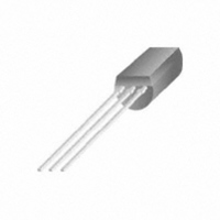
FQNL1N50BBU Fairchild Semiconductor, FQNL1N50BBU Datasheet

FQNL1N50BBU
Specifications of FQNL1N50BBU
Related parts for FQNL1N50BBU
FQNL1N50BBU Summary of contents
Page 1
... T L 1/8" from case for 5 seconds Thermal Characteristics Symbol R Thermal Resistance, Junction-to-Ambient JA ©2001 Fairchild Semiconductor Corporation Features • 0.27A, 500V, R • Low gate charge ( typical 4.0 nC) • Low Crss ( typical 3.0 pF) • Fast switching • Improved dv/dt capability TO-92L FQNL Series T = 25° ...
Page 2
... Repetitive Rating : Pulse width limited by maximum junction temperature ≤ 1.4A, di/dt ≤ 200A/us, V ≤ DSS, 3. Pulse Test : Pulse width ≤ 300us, Duty cycle ≤ Essentially independent of operating temperature ©2001 Fairchild Semiconductor Corporation T = 25°C unless otherwise noted C Test Conditions 250 A GS ...
Page 3
... Drain Current [A] D Figure 3. On-Resistance Variation vs Drain Current and Gate Voltage. 200 C 150 iss C oss 100 50 C rss Drain-Source Voltage [V] DS Figure 5. Capacitance Characteristics. ©2001 Fairchild Semiconductor Corporation ※ Notes : 1. 250μ s Pulse Test 25℃ Figure 2. Transfer Characteristics 10V ※ Note : T = 25℃ ...
Page 4
... 150 Single Pulse - Drain-Source Voltage [V] DS Figure 9. Maximum Safe Operating Area ©2001 Fairchild Semiconductor Corporation (Continued) 3.0 2.5 2.0 1.5 1.0 ※ Note : 0.5 = 250 μ 0.0 100 150 200 -100 o C] Figure 8. On-Resistance Variation 0.30 0. 100 s 0. 100 ms 0.15 0.10 ...
Page 5
... 3mA 3mA Resistive Switching Test Circuit & Waveforms 10V 10V ©2001 Fairchild Semiconductor Corporation Gate Charge Test Circuit & Waveform Same Type Same Type as DUT as DUT 10V 10V DUT DUT 10% ...
Page 6
... Peak Diode Recovery dv/dt Test Circuit & Waveform Driver ) ( Driver ) DUT ) ( DUT ) DUT ) ( DUT ) ©2001 Fairchild Semiconductor Corporation + + DUT DUT Driver Driver Same Type Same Type as DUT as DUT • dv/dt controlled by R • dv/dt controlled by R • I • I controlled by pulse period ...
Page 7
... Package Dimensions 4.90 0.50 0.10 3.90 ©2001 Fairchild Semiconductor Corporation TO-92L 0.20 0.70MAX. 0.80 0.10 1.00MAX. 1.27TYP [1.27 ] 0.20 2.54 TYP 0.20 0.45 0.10 Rev. A, March 2001 ...
Page 8
... TRADEMARKS The following are registered and unregistered trademarks Fairchild Semiconductor owns or is authorized to use and is not intended exhaustive list of all such trademarks. ACEx™ FAST Bottomless™ FASTr™ CoolFET™ FRFET™ CROSSVOLT™ GlobalOptoisolator™ DenseTrench™ GTO™ ...


