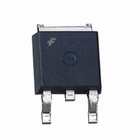
FDD8876 Fairchild Semiconductor, FDD8876 Datasheet - Page 2

FDD8876
Manufacturer Part Number
FDD8876
Description
MOSFET N-CH 30V 73A D-PAK
Manufacturer
Fairchild Semiconductor
Series
PowerTrench®r
Datasheet
1.FDD8876.pdf
(11 pages)
Specifications of FDD8876
Fet Type
MOSFET N-Channel, Metal Oxide
Fet Feature
Logic Level Gate
Rds On (max) @ Id, Vgs
8.2 mOhm @ 35A, 10V
Drain To Source Voltage (vdss)
30V
Current - Continuous Drain (id) @ 25° C
73A
Vgs(th) (max) @ Id
2.5V @ 250µA
Gate Charge (qg) @ Vgs
47nC @ 10V
Input Capacitance (ciss) @ Vds
1700pF @ 15V
Power - Max
70W
Mounting Type
Surface Mount
Package / Case
DPak, TO-252 (2 leads+tab), SC-63
Configuration
Single
Transistor Polarity
N-Channel
Resistance Drain-source Rds (on)
0.011 Ohms
Drain-source Breakdown Voltage
30 V
Gate-source Breakdown Voltage
+/- 20 V
Continuous Drain Current
73 A
Power Dissipation
70 W
Maximum Operating Temperature
+ 175 C
Mounting Style
SMD/SMT
Fall Time
37 ns
Minimum Operating Temperature
- 55 C
Rise Time
91 ns
Lead Free Status / RoHS Status
Lead free / RoHS Compliant
Available stocks
Company
Part Number
Manufacturer
Quantity
Price
Company:
Part Number:
FDD8876
Manufacturer:
FAIRCHILD
Quantity:
30 000
©2008 Fairchild Semiconductor Corporation
Package Marking and Ordering Information
Electrical Characteristics
Off Characteristics
On Characteristics
Dynamic Characteristics
Switching Characteristics
Drain-Source Diode Characteristics
Notes:
1: Package current limitation is 35A.
2: Starting T
3
B
I
I
V
r
C
C
C
R
Q
Q
Q
Q
Q
Q
t
t
t
t
t
t
V
t
Q
DSS
GSS
ON
d(ON)
r
d(OFF)
f
OFF
rr
DS(ON)
GS(TH)
VDSS
SD
ISS
OSS
RSS
G
g(TOT)
g(5)
g(TH)
gs
gs2
gd
RR
Symbol
Device Marking
FDD8876
FDU8876
F
F
J
= 25°C, L = 0.24mH, I
Drain to Source Breakdown Voltage
Zero Gate Voltage Drain Current
Gate to Source Leakage Current
Gate to Source Threshold Voltage
Drain to Source On Resistance
Input Capacitance
Output Capacitance
Reverse Transfer Capacitance
Gate Resistance
Total Gate Charge at 10V
Total Gate Charge at 5V
Threshold Gate Charge
Gate to Source Gate Charge
Gate Charge Threshold to Plateau
Gate to Drain “Miller” Charge
Turn-On Time
Turn-On Delay Time
Rise Time
Turn-Off Delay Time
Fall Time
Turn-Off Time
Source to Drain Diode Voltage
Reverse Recovery Time
Reverse Recovered Charge
AS
Parameter
= 28A, V
FDD8876
FDU8876
Device
(V
DD
GS
= 27V, V
= 10V)
T
C
= 25°C unless otherwise noted
GS
= 10V.
TO-252AA
TO-251AA
Package
V
V
V
I
I
V
V
V
I
I
I
T
V
f = 1MHz
V
V
V
V
I
I
I
D
D
D
D
SD
SD
SD
SD
J
DS
GS
GS
GS
DS
GS
GS
GS
GS
DD
GS
= 250 A, V
= 35A, V
= 35A, V
= 35A, V
= 175
= 35A
= 15A
= 35A, dI
= 35A, dI
= 24V
= 0V
= 20V
= V
= 15V, V
= 0.5V, f = 1MHz
= 0V to 10V
= 0V to 5V
= 0V to 1V
= 15V, I
= 10V, R
Test Conditions
DS
o
C
, I
GS
GS
GS
D
D
SD
SD
GS
GS
GS
= 35A
= 10V
= 4.5V
= 10V,
= 250 A
/dt = 100A/ s
/dt = 100A/ s
Reel Size
= 0V,
= 0V
= 10
T
V
I
I
D
g
Tube
C
DD
13”
= 1.0mA
= 35A
= 150
= 15V
o
C
Tape Width
Min
1.2
30
-
-
-
-
-
-
-
-
-
-
-
-
-
-
-
-
-
-
-
-
-
-
-
-
-
-
12mm
N/A
0.0066 0.0082
0.008
0.011
1700
330
200
Typ
2.2
1.4
4.2
2.8
8.0
34
18
91
44
37
8
-
-
-
-
-
-
-
-
-
-
-
0.010
0.013
1.25
FDD8876 / FDU8876 Rev. A3
Max
250
149
122
2.5
1.9
1.0
100
2500 units
47
26
26
12
Quantity
1
-
-
-
-
-
-
-
-
-
-
-
-
75 units
Units
nC
nC
nC
nC
nC
nC
nC
nA
pF
pF
pF
ns
ns
ns
ns
ns
ns
ns
V
V
V
V
A


