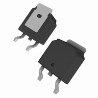
IRLR110TRLPBF Vishay, IRLR110TRLPBF Datasheet - Page 7

IRLR110TRLPBF
Manufacturer Part Number
IRLR110TRLPBF
Description
MOSFET N-CH 100V 4.3A DPAK
Manufacturer
Vishay
Datasheet
1.IRLR110TRL.pdf
(8 pages)
Specifications of IRLR110TRLPBF
Fet Type
MOSFET N-Channel, Metal Oxide
Fet Feature
Logic Level Gate
Rds On (max) @ Id, Vgs
540 mOhm @ 2.6A, 5V
Drain To Source Voltage (vdss)
100V
Current - Continuous Drain (id) @ 25° C
4.3A
Vgs(th) (max) @ Id
2V @ 250µA
Gate Charge (qg) @ Vgs
6.1nC @ 5V
Input Capacitance (ciss) @ Vds
250pF @ 25V
Power - Max
2.5W
Mounting Type
Surface Mount
Package / Case
DPak, TO-252 (2 leads+tab), SC-63
Transistor Polarity
N Channel
Continuous Drain Current Id
4.3A
Drain Source Voltage Vds
100V
On Resistance Rds(on)
540mohm
Rds(on) Test Voltage Vgs
5V
Leaded Process Compatible
Yes
Lead Free Status / RoHS Status
Lead free / RoHS Compliant
Vishay Siliconix maintains worldwide manufacturing capability. Products may be manufactured at one of several qualified locations. Reliability data for Silicon
Technology and Package Reliability represent a composite of all qualified locations. For related documents such as package/tape drawings, part marking, and
reliability data, see www.vishay.com/ppg?91323.
Document Number: 91323
S10-1139-Rev. C, 17-May-10
Re-applied
voltage
Reverse
recovery
current
+
-
R
g
D.U.T.
Note
a. V
Driver gate drive
D.U.T. l
D.U.T. V
Inductor current
GS
= 5 V for logic level devices
P.W.
SD
DS
waveform
waveform
Peak Diode Recovery dV/dt Test Circuit
Ripple ≤ 5 %
Body diode forward drop
Period
Body diode forward
IRLR110, IRLU110, SiHLR110, SiHLU110
+
-
Fig. 14 - For N-Channel
• dV/dt controlled by R
• Driver same type as D.U.T.
• I
• D.U.T. - device under test
Diode recovery
current
SD
controlled by duty factor “D”
Circuit layout considerations
dV/dt
• Low stray inductance
• Ground plane
• Low leakage inductance
current transformer
dI/dt
D =
-
g
Period
P.W.
+
V
I
V
SD
GS
DD
= 10 V
+
-
V
DD
a
Vishay Siliconix
www.vishay.com
7


