FDP3682 Fairchild Semiconductor, FDP3682 Datasheet - Page 4
FDP3682
Manufacturer Part Number
FDP3682
Description
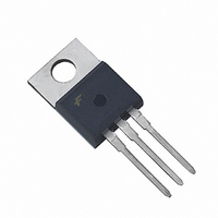
MOSFET N-CH 100V 32A TO-220AB
Manufacturer
Fairchild Semiconductor
Series
PowerTrench®r
Datasheet
1.FDB3682.pdf
(11 pages)
Specifications of FDP3682
Fet Type
MOSFET N-Channel, Metal Oxide
Fet Feature
Standard
Rds On (max) @ Id, Vgs
36 mOhm @ 32A, 10V
Drain To Source Voltage (vdss)
100V
Current - Continuous Drain (id) @ 25° C
32A
Vgs(th) (max) @ Id
4V @ 250µA
Gate Charge (qg) @ Vgs
28nC @ 10V
Input Capacitance (ciss) @ Vds
1250pF @ 25V
Power - Max
95W
Mounting Type
Through Hole
Package / Case
TO-220-3 (Straight Leads)
Configuration
Single
Transistor Polarity
N-Channel
Resistance Drain-source Rds (on)
0.036 Ohm @ 10 V
Drain-source Breakdown Voltage
100 V
Gate-source Breakdown Voltage
+/- 20 V
Continuous Drain Current
6 A
Power Dissipation
95000 mW
Maximum Operating Temperature
+ 175 C
Mounting Style
Through Hole
Minimum Operating Temperature
- 55 C
Lead Free Status / RoHS Status
Lead free / RoHS Compliant
Available stocks
Company
Part Number
Manufacturer
Quantity
Price
Company:

Part Number:
FDP3682
Manufacturer:
FAIRCHILD
Quantity:
12 500
Part Number:
FDP3682
Manufacturer:
FSC
Quantity:
20 000


©2010 Fairchild Semiconductor Corporation
FDB3682/FDP3682 Rev.B1
Typical Characteristics
Figure 9. Drain to Source On Resistance vs Drain
100
200
Figure 5. Forward Bias Safe Operating Area
0.1
10
80
60
40
20
60
50
40
30
20
1
0
3.5
1
0
Figure 7. Transfer Characteristics
PULSE DURATION = 80ms
DUTY CYCLE = 0.5% MAX
PULSE DURATION = 80 s
DUTY CYCLE = 0.5% MAX
V
T
T
OPERATION IN THIS
SINGLE PULSE
LIMITED BY r
DD
J
C
= MAX RATED
= 25
= 15V
4.0
T
AREA MAY BE
5
J
o
= 25
V
C
V
DS
GS
4.5
, DRAIN TO SOURCE VOLTAGE (V)
o
, GATE TO SOURCE VOLTAGE (V)
C
10
DS(ON)
Id, DRAIN CURRENT (A)
Current
T
5.0
J
= 175
10
15
5.5
o
C
T
VGS = 6V
J
20
VGS = 10V
= -55
10ms
DC
6.0
T
C
1ms
o
C
= 25°C unless otherwise noted
25
100 s
6.5
100
30
7.0
10 s
200
7.5
35
NOTE: Refer to Fairchild Application Notes AN7514 and AN7515
100
4
10
80
60
40
20
1
0
Figure 10. Normalized Drain to Source On
Figure 6. Unclamped Inductive Switching
3.0
2.5
2.0
1.5
1.0
0.5
0.001
0
Resistance vs Junction Temperature
Figure 8. Saturation Characteristics
-80
PULSE DURATION = 80 s
DUTY CYCLE = 0.5% MAX
If R = 0
t
If R
t
T
AV
AV
PULSE DURATION = 80 s
DUTY CYCLE = 0.5% MAX
C
= (L)(I
= (L/R)ln[(I
= 25
STARTING T
0
-40
o
C
AS
V
DS
0.01
T
)/(1.3*RATED BV
1
J
t
, DRAIN TO SOURCE VOLTAGE (V)
, JUNCTION TEMPERATURE (
AV
AS
, TIME IN AVALANCHE (ms)
0
*R)/(1.3*RATED BV
Capability
J
= 150
40
o
C
V
0.1
DSS
2
GS
= 20V
- V
80
DD
STARTING T
DSS
)
V
- V
GS
www.fairchildsemi.com
120
DD
= 10V, I
o
1
3
) +1]
C)
V
J
V
V
GS
GS
GS
160
= 25
D
=32A
= 10V
= 6V
= 5V
o
C
200
10
4
Related parts for FDP3682
Image
Part Number
Description
Manufacturer
Datasheet
Request
R

Part Number:
Description:
Fairchild Semiconductor [IGBT MODULE]
Manufacturer:
Fairchild Semiconductor
Datasheet:

Part Number:
Description:
Discrete Semiconductor Modules
Manufacturer:
Fairchild Semiconductor
Part Number:
Description:
Discrete Semiconductor Modules
Manufacturer:
Fairchild Semiconductor
Part Number:
Description:
This N-Channel MOSFET is produced using Fairchild Semiconductor’s advanced Power Trench® process
Manufacturer:
Fairchild Semiconductor
Datasheet:
Part Number:
Description:
This N-Channel MOSFET is produced using Fairchild Semiconductor’s advanced Power Trench® process
Manufacturer:
Fairchild Semiconductor
Datasheet:
Part Number:
Description:
This N-Channel MOSFET is produced using Fairchild Semiconductor’s advanced PowerTrench® process
Manufacturer:
Fairchild Semiconductor
Datasheet:
Part Number:
Description:
This N-Channel MOSFET is produced using Fairchild Semiconductor’s advanced PowerTrench® process
Manufacturer:
Fairchild Semiconductor
Datasheet:
Part Number:
Description:
This N-Channel MOSFET is produced using Fairchild Semiconductor’s advanced Power Trench® process
Manufacturer:
Fairchild Semiconductor
Datasheet:
Part Number:
Description:
This N-Channel logic Level MOSFETs are produced using Fairchild Semiconductor‘s advanced Power Trench® process that has been special tailored to minimize the on-state resistance and yet maintain superior switching performance
Manufacturer:
Fairchild Semiconductor
Datasheet:
Part Number:
Description:
This N-Channel MOSFET is produced using Fairchild Semiconductor’s advanced Power Trench® process
Manufacturer:
Fairchild Semiconductor
Datasheet:
Part Number:
Description:
This N-Channel SyncFET™ is produced using Fairchild Semiconductor’s advanced PowerTrench® process
Manufacturer:
Fairchild Semiconductor
Datasheet:
Part Number:
Description:
This N-Channel SyncFET™ is produced using Fairchild Semiconductor’s advanced PowerTrench® process
Manufacturer:
Fairchild Semiconductor
Datasheet:
Part Number:
Description:
This N-Channel SyncFET™ is produced using Fairchild Semiconductor’s advanced PowerTrench® process
Manufacturer:
Fairchild Semiconductor
Datasheet:
Part Number:
Description:
This N-Channel logic Level MOSFETs are produced using Fairchild Semiconductor‘s advanced Power Trench® process that has been special tailored to minimize the on-state resistance and yet maintain superior switching performance
Manufacturer:
Fairchild Semiconductor
Datasheet:
Part Number:
Description:
This N-Channel MOSFET is produced using Fairchild Semiconductor’s advanced Power Trench® process that has been especially tailored to minimize the on-state resistance and yet maintain superior switching performance
Manufacturer:
Fairchild Semiconductor
Datasheet: