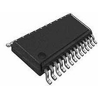
WM8196SCDS Wolfson Microelectronics, WM8196SCDS Datasheet - Page 28

WM8196SCDS
Manufacturer Part Number
WM8196SCDS
Description
Video ICs 16-Bit 12MSPS 3-Channel AFE
Manufacturer
Wolfson Microelectronics
Type
CCD/CISr
Datasheet
1.WM8196SCDS.pdf
(32 pages)
Specifications of WM8196SCDS
Operating Supply Voltage
3.3 V or 5 V
Supply Current
60 mA
Maximum Operating Temperature
+ 70 C
Package / Case
SSOP-28
Conversion Rate
12000 KSPS
Minimum Operating Temperature
- 40 C
Mounting Style
SMD/SMT
Number Of Channels
3
Resolution
16 bit
Lead Free Status / RoHS Status
Lead free / RoHS Compliant
Available stocks
Company
Part Number
Manufacturer
Quantity
Price
Company:
Part Number:
WM8196SCDS
Manufacturer:
Wolfson
Quantity:
6 000
Part Number:
WM8196SCDS
Manufacturer:
WM
Quantity:
20 000
Company:
Part Number:
WM8196SCDS/R
Manufacturer:
PANASONIC
Quantity:
66 562
Part Number:
WM8196SCDS/R
Manufacturer:
WOLFSON
Quantity:
20 000
Part Number:
WM8196SCDS/RV
Manufacturer:
WOLFSON
Quantity:
20 000
WM8196
w
Setup
Register 4
Setup
Register 5
Setup
Register 6
REGISTER
BIT
5:4
7:6
3:1
7:5
3:0
7:4
NO
0
1
2
3
0
4
LINEBYLINE
SELDIS[3:0]
ACYCNRLC
POSNNEG
VSMPDET
VDEL[2:0]
INTM[1:0]
Reserved
Reserved
NAME(S)
RLCINT
FM[1:0]
FME
BIT
DEFAULT
0000
0000
000
000
00
00
0
0
0
0
0
0
Selects line by line operation 0 = normal operation,
1 = line by line operation.
When line by line operation is selected MONO is forced to 1 and CHAN[1:0] to
00 internally, ensuring that the correct internal timing signals are produced.
Green and Blue PGAs are also disabled to save power.
When LINEBYLINE = 0 this bit has no effect.
When LINEBYLINE = 1 this bit determines the function of the RLC/ACYC
input pin and the input multiplexer and offset/gain register controls.
0 = RLC/ACYC pin enabled for Reset Level Clamp. Internal selection of input
and gain/offset multiplexers,
1 = Auto-cycling enabled by pulsing the RLC/ACYC input pin.
See Table 4, Colour Selection Description in Line-by-Line Mode for colour
selection mode details.
When auto-cycling is enabled, the RLC/ACYC pin cannot be used for reset
level clamping. The RLCINT bit may be used instead.
When LINEBYLINE = 0 this bit has no effect.
When LINEBYLINE = 1 this bit controls the input force mux mode:
0 = No force mux, 1 = Force mux mode. Forces the input mux to be selected
by FM[1:0] separately from gain and offset multiplexers.
See Table 4 for details.
When LINEBYLINE = 1 and ACYCNRLC = 1 this bit is used to determine
whether Reset Level Clamping is used.
0 = RLC disabled, 1 = RLC enabled.
Colour selection bits used in internal modes.
00 = Red, 01 = Green, 10 = Blue and 11 = Reserved.
See Table 4 for details.
Colour selection bits used in input force mux modes.
00 = RINP, 01 = GINP, 10 = BINP and 11 = Reserved.
See Table 4 for details.
0 = Normal operation, signal on VSMP input pin is applied directly to Timing
Control block.
1 = Programmable VSMP detect circuit is enabled. An internal synchronisation
pulse is generated from signal applied to VSMP input pin and is applied to
Timing Control block.
When VSMPDET = 0 these bits have no effect.
When VSMPDET = 1 these bits set a programmable delay from the detected
edge of the signal applied to the VSMP pin. The internally generated pulse is
delayed by VDEL MCLK periods from the detected edge.
See Figure 19, Internal VSMP Pulses Generated for details.
When VSMPDET = 0 this bit has no effect.
When VSMPDET = 1 this bit controls whether positive or negative edges
are detected:
0 = Negative edge on VSMP pin is detected and used to generate internal
timing pulse.
1 = Positive edge on VSMP pin is detected and used to generate internal
timing pulse.
See Figure 19 for further details.
Must be set to zero
Selective power disable register - activated when SELPD = 1.
Each bit disables respective cell when 1, enabled when 0.
SELDIS[0] = Red CDS, PGA
SELDIS[1] = Green CDS, PGA
SELDIS[2] = Blue CDS, PGA
SELDIS[3] = ADC
Must be set to zero
DESCRIPTION
PD Rev 4.3 March 2007
Production Data
28


