IRFL9014TRPBF Vishay, IRFL9014TRPBF Datasheet - Page 2
IRFL9014TRPBF
Manufacturer Part Number
IRFL9014TRPBF
Description
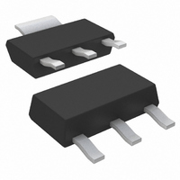
MOSFET P-CH 60V 1.8A SOT223
Manufacturer
Vishay
Datasheet
1.IRFL9014TRPBF.pdf
(9 pages)
Specifications of IRFL9014TRPBF
Fet Type
MOSFET P-Channel, Metal Oxide
Fet Feature
Standard
Rds On (max) @ Id, Vgs
500 mOhm @ 1.1A, 10V
Drain To Source Voltage (vdss)
60V
Current - Continuous Drain (id) @ 25° C
1.8A
Vgs(th) (max) @ Id
4V @ 250µA
Gate Charge (qg) @ Vgs
12nC @ 10V
Input Capacitance (ciss) @ Vds
270pF @ 25V
Power - Max
2W
Mounting Type
Surface Mount
Package / Case
SOT-223 (3 leads + Tab), SC-73, TO-261
Minimum Operating Temperature
- 55 C
Configuration
Single Dual Drain
Transistor Polarity
P-Channel
Resistance Drain-source Rds (on)
0.5 Ohm @ 10 V
Drain-source Breakdown Voltage
60 V
Gate-source Breakdown Voltage
+/- 20 V
Continuous Drain Current
1.8 A
Power Dissipation
2000 mW
Maximum Operating Temperature
+ 150 C
Mounting Style
SMD/SMT
Lead Free Status / RoHS Status
Lead free / RoHS Compliant
Lead Free Status / RoHS Status
Lead free / RoHS Compliant, Lead free / RoHS Compliant
Other names
IRFL9014PBFTR
Available stocks
Company
Part Number
Manufacturer
Quantity
Price
Company:

Part Number:
IRFL9014TRPBF
Manufacturer:
ATMEL
Quantity:
1 001
Part Number:
IRFL9014TRPBF
Manufacturer:
VISHAY/威世
Quantity:
20 000


IRFL9014PbF
Electrical Characteristics @ T
Document Number: 91195
‚
Source-Drain Ratings and Characteristics
Notes:
I
I
V
t
Q
t
∆V
L
SM
V
L
S
rr
on
GSS
V
g
Q
Q
Q
t
t
t
t
C
C
C
DSS
d(on)
r
d(off)
f
SD
D
rr
S
(BR)DSS
fs
Repetitive rating; pulse width limited by
max. junction temperature. ( See fig. 11 )
GS(th)
DS(on)
iss
oss
rss
g
gs
gd
V
(BR)DSS
R
DD=
G
= 25Ω, I
-25V, starting T
/∆T
J
Continuous Source Current
(Body Diode)
Pulsed Source Current
(Body Diode)
Diode Forward Voltage
Reverse Recovery Time
Reverse RecoveryCharge
Forward Turn-On Time
Breakdown Voltage Temp. Coefficient
Drain-to-Source Breakdown Voltage
Internal Drain Inductance
Gate Threshold Voltage
Forward Transconductance
Gate-to-Source Forward Leakage
Gate-to-Source Reverse Leakage
Total Gate Charge
Gate-to-Source Charge
Gate-to-Drain ("Miller") Charge
Turn-On Delay Time
Rise Time
Turn-Off Delay Time
Input Capacitance
Output Capacitance
Reverse Transfer Capacitance
AS
Internal Source Inductance
Fall Time
= -1.8A. (See Figure 12)
J
= 25°C, L =50 mH
Parameter
Parameter
J
= 25°C (unless otherwise specified)
ƒ
„
T
Pulse width ≤ 300µs; duty cycle ≤ 2%.
I
–––
Min. Typ. Max. Units
–––
SD
–––
–––
––– 0.096 0.19
–––
-2.0
–––
–––
–––
–––
–––
–––
–––
–––
–––
–––
–––
–––
-60
–––
–––
1.3
–––
J
Min. Typ. Max. Units
≤ 150°C
Intrinsic turn-on time is negligible (turn-on is dominated by L
≤
-0.059 –––
–––
–––
80
––– 0.50
–––
–––
––– -100
––– -500
–––
–––
–––
–––
270
170
––– -100
9.6
4.0
11
63
31
6.0
31
, di/dt ≤90A/µs, V
-5.5
160
–––
-4.0
–––
100
–––
–––
–––
–––
–––
–––
–––
3.8
5.1
–––
12
–––
V/°C
µC
ns
V
nC
nH
µA
nA
pF
ns
V
Ω
V
S
Between lead, 6mm(0.25in)
from package and center
of die contact.
showing the
MOSFET symbol
integral reverse
p-n junction diode.
T
T
di/dt = 100A/µs „
Reference to 25°C, I
DD
V
V
V
V
V
V
V
V
I
V
V
V
I
R
V
V
ƒ = 1.0MHz, See Fig. 5
D
D
R
J
J
GS
GS
DS
DS
DS
DS
GS
GS
DS
GS
DD
GS
DS
G
= 25°C, I
= 25°C, I
D
=-6.7A
= -6.7A
≤ V
= 24 Ω
= 4.0 Ω,
= 0V, I
= V
= -25V, I
= -60V, V
= -48V, V
=-48V
= -30V
= 25V
= -10V, I
= -20V
= 20V
= -10V, See Fig. 6 and 13 „
= 0V
(BR)DSS
GS
, I
S
F
D
Conditions
D
=-6.7A
= -1.8A, V
= 250µA
Conditions
D
,
D
GS
GS
= 250µA
= 1.1A „
= 1.1A „
See Fig. 10 „
= 0V
= 0V, T
D
www.vishay.com
= 1mA
GS
J
= 125°C
= 0V „
G
S
+L
G
D
)
D
S
S
D
2
Related parts for IRFL9014TRPBF
Image
Part Number
Description
Manufacturer
Datasheet
Request
R

Part Number:
Description:
MOSFET P-CH 60V 1.8A SOT223
Manufacturer:
Vishay
Datasheet:

Part Number:
Description:
357-036-542-201 CARDEDGE 36POS DL .156 BLK LOPRO
Manufacturer:
Vishay
Datasheet:
Part Number:
Description:
357-036-542-201 CARDEDGE 36POS DL .156 BLK LOPRO
Manufacturer:
Vishay
Datasheet:
Part Number:
Description:
357-036-542-201 CARDEDGE 36POS DL .156 BLK LOPRO
Manufacturer:
Vishay
Datasheet:
Part Number:
Description:
357-036-542-201 CARDEDGE 36POS DL .156 BLK LOPRO
Manufacturer:
Vishay
Datasheet:
Part Number:
Description:
357-036-542-201 CARDEDGE 36POS DL .156 BLK LOPRO
Manufacturer:
Vishay
Datasheet:
Part Number:
Description:
357-036-542-201 CARDEDGE 36POS DL .156 BLK LOPRO
Manufacturer:
Vishay
Datasheet:
Part Number:
Description:
357-036-542-201 CARDEDGE 36POS DL .156 BLK LOPRO
Manufacturer:
Vishay
Datasheet:
Part Number:
Description:
357-036-542-201 CARDEDGE 36POS DL .156 BLK LOPRO
Manufacturer:
Vishay
Datasheet:
Part Number:
Description:
357-036-542-201 CARDEDGE 36POS DL .156 BLK LOPRO
Manufacturer:
Vishay
Datasheet:
Part Number:
Description:
357-036-542-201 CARDEDGE 36POS DL .156 BLK LOPRO
Manufacturer:
Vishay
Datasheet:
Part Number:
Description:
357-036-542-201 CARDEDGE 36POS DL .156 BLK LOPRO
Manufacturer:
Vishay
Datasheet:
Part Number:
Description:
357-036-542-201 CARDEDGE 36POS DL .156 BLK LOPRO
Manufacturer:
Vishay
Datasheet:
Part Number:
Description:
357-036-542-201 CARDEDGE 36POS DL .156 BLK LOPRO
Manufacturer:
Vishay
Datasheet:
Part Number:
Description:
357-036-542-201 CARDEDGE 36POS DL .156 BLK LOPRO
Manufacturer:
Vishay
Datasheet: