FQA13N50CF Fairchild Semiconductor, FQA13N50CF Datasheet

MOSFET N-CH 500V 15A TO-3P

FQA13N50CF

Manufacturer Part Number
FQA13N50CF
Description
MOSFET N-CH 500V 15A TO-3P
Manufacturer
Fairchild Semiconductor
Series
FRFET™r
Datasheet

Specifications of FQA13N50CF

Fet Type
MOSFET N-Channel, Metal Oxide
Fet Feature
Standard
Rds On (max) @ Id, Vgs
480 mOhm @ 7.5A, 10V
Drain To Source Voltage (vdss)
500V
Current - Continuous Drain (id) @ 25° C
15A
Vgs(th) (max) @ Id
4V @ 250µA
Gate Charge (qg) @ Vgs
56nC @ 10V
Input Capacitance (ciss) @ Vds
2055pF @ 25V
Power - Max
218W
Mounting Type
Through Hole
Package / Case
TO-3PN-3
Configuration
Single
Transistor Polarity
N-Channel
Resistance Drain-source Rds (on)
0.48 Ohms
Drain-source Breakdown Voltage
500 V
Gate-source Breakdown Voltage
+/- 30 V
Continuous Drain Current
15 A
Power Dissipation
218 W
Maximum Operating Temperature
+ 150 C
Mounting Style
Through Hole
Minimum Operating Temperature
- 55 C
Lead Free Status / RoHS Status
Lead free / RoHS Compliant

Available stocks

Company
Part Number
Manufacturer
Quantity
Price
Part Number:
FQA13N50CF
Manufacturer:
FSC
Quantity:
21 000
Part Number:
FQA13N50CF
Manufacturer:
FAIRCHILD
Quantity:
8 000
Part Number:
FQA13N50CF
Manufacturer:
FAIRCHILD/仙童
Quantity:
20 000
©2007 Fairchild Semiconductor Corporation
FQA13N50CF Rev. A1
FQA13N50CF
500V N-Channel MOSFET
Features
• 15A, 500V, R
• Low gate charge (typical 43nC)
• Low C
• Fast switching
• 100% avalanche tested
• Improved dv/dt capability
• Fast recovery body diode (typical 100ns)
• RoHS compliant
Absolute Maximum Ratings
Thermal Characteristics
V
I
I
V
E
I
E
dv/dt
P
T
T
R
R
R
D
DM
AR
J
L
DSS
GSS
AS
AR
D
θJC
θJS
θJA
, T
Symbol
Symbol
STG
rss
(typical 20pF)
DS(on)
Thermal Resistance, Junction-to-Case
Thermal Resistance, Case-to-Sink
Thermal Resistance, Junction-to-Ambient
Drain-Source Voltage
Drain Current
Drain Current
Gate-Source Voltage
Single Pulsed Avalanche Energy
Avalanche Current
Repetitive Avalanche Energy
Peak Diode Recovery dv/dt
Power Dissipation (T
Operating and Storage Temperature Range
Maximum lead temperature for soldering purposes,
1/8''"from case for 5 seconds
= 0.48Ω @V
G
D
S
GS
= 10 V
- Continuous (T
- Continuous (T
- Pulsed
- Derate above 25°C
TO-3PN
FQA Series
C
= 25°C)
Parameter
Parameter
C
C
= 25°C)
= 100°C)
1
Description
These N-Channel enhancement mode power field effect
transistors are produced using Fairchild’s proprietary, planar
stripe, DMOS technology.
This advanced technology has been especially tailored to
minimize on-state resistance, provide superior switching
performance, and withstand high energy pulse in the avalanche
and commutation mode. These devices are well suited for high
efficient switched mode power supplies, active power factor
correction, electronic lamp ballast based on half bridge
topology.
(Note 1)
(Note 2)
(Note 1)
(Note 1)
(Note 3)
G
Typ
0.24
--
--
FQA13N50CF
-55 to +150
S
D
± 30
21.8
1.56
500
860
218
300
9.5
4.5
15
60
15
Max
0.58
FRFET
40
--
July 2007
www.fairchildsemi.com
Units
W/°C
Units
V/ns
°C/W
°C/W
°C/W
mJ
mJ
°C
°C
W
V
A
A
A
V
A
®

Related parts for FQA13N50CF

FQA13N50CF Summary of contents

Page 1

... Thermal Resistance, Case-to-Sink θJS R Thermal Resistance, Junction-to-Ambient θJA ©2007 Fairchild Semiconductor Corporation FQA13N50CF Rev. A1 Description = 10 V These N-Channel enhancement mode power field effect transistors are produced using Fairchild’s proprietary, planar stripe, DMOS technology. This advanced technology has been especially tailored to ...

Page 2

... L = 5.6mH, I =15A 50V ≤ 15A, di/dt ≤200A/µs, V ≤ Starting DSS, 4. Pulse Test : Pulse width ≤ 300µs, Duty cycle ≤ Essentially independent of operating temperature FQA13N50CF Rev. A1 Package Reel Size TO-3PN -- TO-3PN -- T = 25°C unless otherwise noted C Test Conditions = 250 µ 250 µ ...

Page 3

... Drain Current and Gate Voltage 1.5 1.0 0 Drain Current [A] D Figure 5. Capacitance Characteristics 3000 2500 C iss 2000 C oss 1500 1000 C rss 500 Drain-Source Voltage [V] DS FQA13N50CF Rev. A1 Figure 2. Transfer Characteristics 10 10 Notes : 1. 250us Pulse Test ° Figure 4. Body Diode Forward Voltage 10V 20V GS ° Note : Figure 6 ...

Page 4

... DS(on 100 Notes : ° ° 150 Single Pulse - Drain-Source Voltage [V] DS Figure 11. Transient Thermal Response Curve FQA13N50CF Rev. A1 (Continued) Figure 8. On-Resistance Variation Notes : µ 250 A D 100 150 200 ° C] Figure 10. Maximum Drain Current µ µ 100 vs. Temperature 3.0 2.5 2.0 1 ...

Page 5

... Unclamped Inductive Switching Test Circuit & Waveforms FQA13N50CF Rev. A1 Gate Charge Test Circuit & Waveform Resistive Switching Test Circuit & Waveforms 5 www.fairchildsemi.com ...

Page 6

... FQA13N50CF Rev. A1 Peak Diode Recovery dv/dt Test Circuit & Waveforms 6 www.fairchildsemi.com ...

Page 7

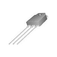
... Mechanical Dimensions FQA13N50CF Rev. A1 TO-3PN 8 Dimensions in Millimeters www.fairchildsemi.com ...

Page 8

... TRADEMARKS The following are registered and unregistered trademarks and service marks Fairchild Semiconductor owns or is authorized to use and is not intended exhaustive list of all such trademarks. ® ACEx Build it Now™ CorePLUS™ CROSSVOLT™ CTL™ Current Transfer Logic™ ® ...

Related keywords