IRF9Z34STRLPBF Vishay, IRF9Z34STRLPBF Datasheet - Page 7
IRF9Z34STRLPBF
Manufacturer Part Number
IRF9Z34STRLPBF
Description
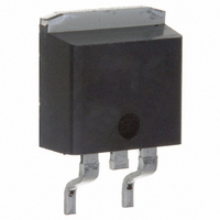
MOSFET P-CH 60V 18A D2PAK
Manufacturer
Vishay
Datasheet
1.IRF9Z34STRLPBF.pdf
(8 pages)
Specifications of IRF9Z34STRLPBF
Transistor Polarity
P-Channel
Fet Type
MOSFET P-Channel, Metal Oxide
Fet Feature
Standard
Rds On (max) @ Id, Vgs
140 mOhm @ 11A, 10V
Drain To Source Voltage (vdss)
60V
Current - Continuous Drain (id) @ 25° C
18A
Vgs(th) (max) @ Id
4V @ 250µA
Gate Charge (qg) @ Vgs
34nC @ 10V
Input Capacitance (ciss) @ Vds
1100pF @ 25V
Power - Max
3.7W
Mounting Type
Surface Mount
Package / Case
D²Pak, TO-263 (2 leads + tab)
Gate Charge Qg
34 nC
Minimum Operating Temperature
- 55 C
Configuration
Single
Resistance Drain-source Rds (on)
0.14 Ohm at 10 V
Forward Transconductance Gfs (max / Min)
5.9 S
Drain-source Breakdown Voltage
60 V
Gate-source Breakdown Voltage
20 V
Continuous Drain Current
18 A
Power Dissipation
3700 mW
Maximum Operating Temperature
+ 175 C
Mounting Style
SMD/SMT
Continuous Drain Current Id
-18A
Drain Source Voltage Vds
-60V
On Resistance Rds(on)
140mohm
Rds(on) Test Voltage Vgs
-10V
Leaded Process Compatible
Yes
Lead Free Status / RoHS Status
Lead free / RoHS Compliant
Lead Free Status / RoHS Status
Lead free / RoHS Compliant, Lead free / RoHS Compliant


Vishay Siliconix maintains worldwide manufacturing capability. Products may be manufactured at one of several qualified locations. Reliability data for Silicon
Technology and Package Reliability represent a composite of all qualified locations. For related documents such as package/tape drawings, part marking, and
reliability data,
Document Number: 91093
S10-1728-Rev. B, 02-Aug-10
see www.vishay.com/ppg?91093.
Re-applied
voltage
Reverse
recovery
current
+
-
R
g
D.U.T.
Note
• Compliment N-Channel of D.U.T. for driver
a. V
Note
Driver gate drive
D.U.T. l
D.U.T. V
Inductor current
GS
IRF9Z34S, SiHF9Z34S, IRF9Z34L, SiHF9Z34L
= - 5 V for logic level and - 3 V drive devices
P.W.
SD
DS
waveform
waveform
Peak Diode Recovery dV/dt Test Circuit
Body diode forward drop
Fig. 14 - For P-Channel
Ripple ≤ 5 %
Period
Body diode forward
+
-
• dV/dt controlled by R
• I
• D.U.T. - device under test
current
SD
Diode recovery
controlled by duty factor “D”
Circuit layout considerations
• Low stray inductance
• Ground plane
• Low leakage inductance
dV/dt
current transformer
dI/dt
D =
-
g
Period
P.W.
+
I
V
V
SD
GS
DD
= - 10 V
+
-
V
DD
a
Vishay Siliconix
www.vishay.com
7
Related parts for IRF9Z34STRLPBF
Image
Part Number
Description
Manufacturer
Datasheet
Request
R

Part Number:
Description:
MOSFET P-CH 60V 18A D2PAK
Manufacturer:
Vishay
Datasheet:

Part Number:
Description:
357-036-542-201 CARDEDGE 36POS DL .156 BLK LOPRO
Manufacturer:
Vishay
Datasheet:
Part Number:
Description:
357-036-542-201 CARDEDGE 36POS DL .156 BLK LOPRO
Manufacturer:
Vishay
Datasheet:
Part Number:
Description:
357-036-542-201 CARDEDGE 36POS DL .156 BLK LOPRO
Manufacturer:
Vishay
Datasheet:
Part Number:
Description:
357-036-542-201 CARDEDGE 36POS DL .156 BLK LOPRO
Manufacturer:
Vishay
Datasheet:
Part Number:
Description:
357-036-542-201 CARDEDGE 36POS DL .156 BLK LOPRO
Manufacturer:
Vishay
Datasheet:
Part Number:
Description:
357-036-542-201 CARDEDGE 36POS DL .156 BLK LOPRO
Manufacturer:
Vishay
Datasheet:
Part Number:
Description:
357-036-542-201 CARDEDGE 36POS DL .156 BLK LOPRO
Manufacturer:
Vishay
Datasheet:
Part Number:
Description:
357-036-542-201 CARDEDGE 36POS DL .156 BLK LOPRO
Manufacturer:
Vishay
Datasheet:
Part Number:
Description:
357-036-542-201 CARDEDGE 36POS DL .156 BLK LOPRO
Manufacturer:
Vishay
Datasheet:
Part Number:
Description:
357-036-542-201 CARDEDGE 36POS DL .156 BLK LOPRO
Manufacturer:
Vishay
Datasheet:
Part Number:
Description:
357-036-542-201 CARDEDGE 36POS DL .156 BLK LOPRO
Manufacturer:
Vishay
Datasheet:
Part Number:
Description:
357-036-542-201 CARDEDGE 36POS DL .156 BLK LOPRO
Manufacturer:
Vishay
Datasheet:
Part Number:
Description:
357-036-542-201 CARDEDGE 36POS DL .156 BLK LOPRO
Manufacturer:
Vishay
Datasheet:
Part Number:
Description:
357-036-542-201 CARDEDGE 36POS DL .156 BLK LOPRO
Manufacturer:
Vishay
Datasheet: