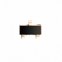
SI2301-TP Micro Commercial Components (MCC), SI2301-TP Datasheet - Page 2

SI2301-TP
Manufacturer Part Number
SI2301-TP
Description
MOSFET P-CH 20V 2.8A SOT-23
Manufacturer
Micro Commercial Components (MCC)
Datasheet
1.SI2301-TP.pdf
(5 pages)
Specifications of SI2301-TP
Fet Type
MOSFET P-Channel, Metal Oxide
Fet Feature
Logic Level Gate
Rds On (max) @ Id, Vgs
120 mOhm @ 2.8A, 4.5V
Drain To Source Voltage (vdss)
20V
Current - Continuous Drain (id) @ 25° C
2.8A
Vgs(th) (max) @ Id
450mV @ 250µA
Gate Charge (qg) @ Vgs
14.5nC @ 4.5V
Input Capacitance (ciss) @ Vds
880pF @ 6V
Power - Max
1.25W
Mounting Type
Surface Mount
Package / Case
SOT-23
Transistor Polarity
P-Channel
Resistance Drain-source Rds (on)
110 mOhms
Forward Transconductance Gfs (max / Min)
8 S
Drain-source Breakdown Voltage
- 20 V
Continuous Drain Current
- 2.8 A
Power Dissipation
1.25 W
Maximum Operating Temperature
+ 150 C
Mounting Style
SMD/SMT
Lead Free Status / RoHS Status
Lead free / RoHS Compliant
Other names
SI2301-TPMSTR
Available stocks
Company
Part Number
Manufacturer
Quantity
Price
Part Number:
SI2301-TP
Manufacturer:
MICRO
Quantity:
20 000
Revision: A
Micro Commercial Components
Electrical Characteristics
M C C
Off Characteristics
Drain-Source Breakdown Voltage
Zero Gate Voltage Drain Current
Gate Body Leakage Current, Forward
Gate Body Leakage Current, Reverse
On Characteristics
Gate Threshold Voltage
Static Drain-Source
On-Resistance
Forward Transconductance
Dynamic Characteristics
Input Capacitance
Output Capacitance
Reverse Transfer Capacitance
Switching Characteristics
Turn-On Delay Time
Turn-On Rise Time
Turn-Off Delay Time
Turn-Off Fall Time
Total Gate Charge
Gate-Source Charge
Gate-Drain Charge
Drain-Source Diode Characteristics and Maximun Ratings
Drain-Source Diode Forward Current
Drain-Source Diode Forward Voltage
Notes :
a.Repetitive Rating : Pulse width limited by maximum junction temperature.
b.Surface Mounted on FR4 Board, t < 5 sec.
c.Pulse Test : Pulse Width < 300µs, Duty Cycle < 2%.
d.Guaranteed by design, not subject to production testing.
Parameter
www.mccsemi.com
c
d
d
TM
b
c
T
A
= 25 C unless otherwise noted
Symbol
R
V
BV
t
t
C
V
I
C
C
Q
I
GS(th)
DS(on)
d(on)
d(off)
Q
g
I
GSSF
Q
GSSR
I
t
DSS
t
SD
oss
FS
iss
rss
S
r
f
gs
gd
DSS
g
2 of 5
V
V
V
V
V
V
V
V
V
f = 1.0 MHz
V
V
V
V
V
GS
DS
GS
GS
GS
GS
GS
DS
DS
DD
GS
DS
GS
GS
Test Condition
= -20V, V
= -5V, I
= -6V, V
= -4.5V, R
= -6V, I
= 0V, I
= 8V, V
= -8V, V
= V
= -4.5V, I
= -2.5V, I
= -6V, I
= -4.5V
= 0V, I
DS
, I
D
S
D
D
D
D
DS
DS
GS
= -0.75A
= -250 µ A
D
D
= -2.8A
= -1A,
= -2.8A,
GS
GEN
= -250 µ A
= 0V
= -2.8A
= -2.0A
= 0V
= 0V,
= 0V
= 6Ω
-0.45
Min
-20
SI2301
Typ
110
880
270
175
1.5
2.1
80
11
32
23
11
8
5
-0.75
-100
Max
14.5
-1.2
120
150
100
20
10
65
45
-1
Units
mΩ
mΩ
µ A
nA
nA
pF
pF
pF
nC
nC
nC
ns
ns
ns
ns
V
V
S
A
V
2011/01/01


