IRF3315SPBF International Rectifier, IRF3315SPBF Datasheet

MOSFET N-CH 150V 21A D2PAK

IRF3315SPBF

Manufacturer Part Number
IRF3315SPBF
Description
MOSFET N-CH 150V 21A D2PAK
Manufacturer
International Rectifier
Series
HEXFET®r
Datasheets

Specifications of IRF3315SPBF

Fet Type
MOSFET N-Channel, Metal Oxide
Fet Feature
Standard
Rds On (max) @ Id, Vgs
82 mOhm @ 12A, 10V
Drain To Source Voltage (vdss)
150V
Current - Continuous Drain (id) @ 25° C
21A
Vgs(th) (max) @ Id
4V @ 250µA
Gate Charge (qg) @ Vgs
95nC @ 10V
Input Capacitance (ciss) @ Vds
1300pF @ 25V
Power - Max
3.8W
Mounting Type
Surface Mount
Package / Case
D²Pak, TO-263 (2 leads + tab)
Current, Drain
21 A
Gate Charge, Total
95 nC
Package Type
D2Pak
Polarization
N-Channel
Power Dissipation
94 W
Resistance, Drain To Source On
0.082 Ohm
Temperature, Operating, Maximum
+175 °C
Temperature, Operating, Minimum
-55 °C
Time, Turn-off Delay
49 ns
Time, Turn-on Delay
9.6 ns
Transconductance, Forward
17 S
Voltage, Breakdown, Drain To Source
150 V
Voltage, Forward, Diode
1.3 V
Voltage, Gate To Source
±20 V
Transistor Polarity
N Channel
Continuous Drain Current Id
21A
Drain Source Voltage Vds
150V
On Resistance Rds(on)
82mohm
Rds(on) Test Voltage Vgs
10V
Threshold Voltage Vgs Typ
4V
Rohs Compliant
Yes
Drain-source Breakdown Voltage
150 V
Gate-source Breakdown Voltage
20 V
Continuous Drain Current
21 A
Mounting Style
SMD/SMT
Gate Charge Qg
63.3 nC
Lead Free Status / RoHS Status
Lead free / RoHS Compliant
Other names
*IRF3315SPBF
Absolute Maximum Ratings
Thermal Resistance
Description
Fifth Generation HEXFETs from International Rectifier
utilize advanced processing techniques to achieve
extremely low
benefit, combined with the fast switching speed and
ruggedized device design that HEXFET Power MOSFETs
are well known for, provides the designer with an extremely
efficient and reliable device for use in a wide variety of
applications.
The D
accommodating die sizes up to HEX-4. It provides the
highest power capability and the lowest possible on-
resistance in any existing surface mount package. The
D
its low internal connection resistance and can dissipate
up to 2.0W in a typical surface mount application.
The through-hole version (IRF3315L) is available for low-
profile applications.
R
R
I
I
I
P
P
V
E
I
E
dv/dt
T
T
AR
D
D
DM
2
AS
AR
J
STG
D
D
GS
Pak is suitable for high current applications because of
JA
@ T
@ T
JC
@T
@T
Advanced Process Technology
Surface Mount (IRF3315S)
Low-profile through-hole (IRF3315L)
175°C Operating Temperature
Fast Switching
Fully Avalanche Rated
2
C
C
Pak is a surface mount power package capable of
A
C
= 25°C
= 25°C
= 100°C
= 25°C
on-resistance per silicon area.
Junction-to-Case
Junction-to-Ambient ( PCB Mounted,steady-state)**
Continuous Drain Current, V
Pulsed Drain Current
Power Dissipation
Power Dissipation
Linear Derating Factor
Gate-to-Source Voltage
Single Pulse Avalanche Energy
Avalanche Current
Repetitive Avalanche Energy
Peak Diode Recovery dv/dt
Operating Junction and
Storage Temperature Range
Soldering Temperature, for 10 seconds
Parameter
Parameter
PRELIMINARY
GS
GS
@ 10V
@ 10V
This
G
Typ.
300 (1.6mm from case )
–––
–––
HEXFET
D P ak
2
-55 to + 175
S
D
IRF3315S/L
Max.
0.63
± 20
350
3.8
9.4
2.5
21
15
84
94
12
®
R
Power MOSFET
DS(on)
V
T O -26 2
Max.
1.6
DSS
40
I
D
= 21A
PD - 9.1617A
= 0.082
= 150V
Units
Units
W/°C
V/ns
°C/W
mJ
mJ
W
W
°C
A
V
A
11/7/97

Related parts for IRF3315SPBF

IRF3315SPBF Summary of contents

Page 1

... Low-profile through-hole (IRF3315L) 175°C Operating Temperature Fast Switching Fully Avalanche Rated Description Fifth Generation HEXFETs from International Rectifier utilize advanced processing techniques to achieve extremely low on-resistance per silicon area. benefit, combined with the fast switching speed and ruggedized device design that HEXFET Power MOSFETs ...

Page 2

IRF3315S/L Electrical Characteristics @ T Parameter V Drain-to-Source Breakdown Voltage (BR)DSS Breakdown Voltage Temp. Coefficient (BR)DSS J R Static Drain-to-Source On-Resistance DS(on) V Gate Threshold Voltage GS(th) g Forward Transconductance fs I Drain-to-Source Leakage Current DSS Gate-to-Source ...

Page 3

VGS TOP 15V 10V 8.0V 7.0V 6.0V 5.5V 5.0V BOTTOM 4.5V 10 4.5V 20µs PULSE WIDTH 0 Drain-to-Source Voltage (V) DS Fig 1. Typical Output Characteristics 100 ° ...

Page 4

IRF3315S/L 3000 iss rss gd 2500 oss ds C iss 2000 1500 C oss 1000 C rss 500 ...

Page 5

T , Case Temperature ( C) C Fig 9. Maximum Drain Current Vs. Case Temperature 0.50 0.20 0.10 0.05 0.1 0.02 0.01 SINGLE PULSE (THERMAL RESPONSE) ...

Page 6

IRF3315S 20V Fig 12a. Unclamped Inductive Test Circuit Fig 12b. Unclamped Inductive Waveforms ...

Page 7

Peak Diode Recovery dv/dt Test Circuit + D.U Driver Gate Drive Period P.W. D.U.T. I Waveform SD Reverse Recovery Body Diode Forward Current D.U.T. V Waveform DS Re-Applied Voltage Body Diode Inductor Curent Ripple * ...

Page 8

IRF3315S Pak Package Outline 10.54 (.415) 10.29 (.405) 1.40 (.055 1.78 (.070) 1.27 (.050 1.40 (.055) 3X 1.14 (.045) 5.08 (.200 ) ...

Page 9

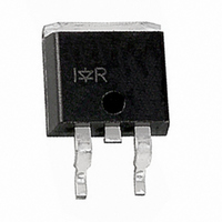
Package Outline TO-262 Outline Part Marking Information TO-262 IRF3315S/L ...

Page 10

IRF3315S/L Tape & Reel Information 2 D Pak TIO 330.00 (14.173 ...

Related keywords