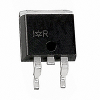
IRF8010SPBF International Rectifier, IRF8010SPBF Datasheet - Page 4

IRF8010SPBF
Manufacturer Part Number
IRF8010SPBF
Description
MOSFET N-CH 100V 80A D2PAK
Manufacturer
International Rectifier
Series
HEXFET®r
Type
Power MOSFETr
Specifications of IRF8010SPBF
Fet Type
MOSFET N-Channel, Metal Oxide
Fet Feature
Standard
Rds On (max) @ Id, Vgs
15 mOhm @ 45A, 10V
Drain To Source Voltage (vdss)
100V
Current - Continuous Drain (id) @ 25° C
80A
Vgs(th) (max) @ Id
4V @ 250µA
Gate Charge (qg) @ Vgs
120nC @ 10V
Input Capacitance (ciss) @ Vds
3830pF @ 25V
Power - Max
260W
Mounting Type
Surface Mount
Package / Case
D²Pak, TO-263 (2 leads + tab)
Current, Drain
80 A
Gate Charge, Total
81 nC
Package Type
D2Pak
Polarization
N-Channel
Power Dissipation
260 W
Resistance, Drain To Source On
12 Milliohms
Temperature, Operating, Maximum
+175 °C
Temperature, Operating, Minimum
-55 °C
Time, Turn-off Delay
61 ns
Time, Turn-on Delay
15 ns
Transconductance, Forward
82 V
Voltage, Breakdown, Drain To Source
100 V
Voltage, Forward, Diode
1.3 V
Voltage, Gate To Source
±20 V
Configuration
Single
Transistor Polarity
N-Channel
Resistance Drain-source Rds (on)
15 m Ohms
Drain-source Breakdown Voltage
100 V
Gate-source Breakdown Voltage
20 V
Continuous Drain Current
80 A
Maximum Operating Temperature
+ 175 C
Mounting Style
SMD/SMT
Fall Time
120 ns
Gate Charge Qg
81 nC
Minimum Operating Temperature
- 55 C
Rise Time
130 ns
Number Of Elements
1
Polarity
N
Channel Mode
Enhancement
Drain-source On-res
0.015Ohm
Drain-source On-volt
100V
Gate-source Voltage (max)
±20V
Operating Temp Range
-55C to 175C
Operating Temperature Classification
Military
Mounting
Surface Mount
Pin Count
2 +Tab
Lead Free Status / RoHS Status
Lead free / RoHS Compliant
Other names
*IRF8010SPBF
IRF8010S/LPbF
Notes:
‚
ƒ
„
…
10
Dimensions are shown in millimeters (inches)
Repetitive rating; pulse width limited by max. junction
Pulse width ≤ 300µs; duty cycle ≤ 2%.
temperature.
I
Rth(jc) (end of life) is the maximum measured value
after 1000 temperature cycles from -55 to 150°C and
is accounted for by the physical wearout of the die attach
medium
material (solder/substrate), process and re-flow
temperature.
2
Starting T
SD
≤ 45A, di/dt ≤ 110A/µs, V
in worse case PCB mounting condition of
J
= 25°C, L = 0.31mH, R
FEED DIRECTION
FEED DIRECTION
NOTES :
1. COMFORMS TO EIA-418.
2. CONTROLLING DIMENSION: MILLIMETER.
3. DIMENSION MEASURED @ HUB.
4. INCLUDES FLANGE DISTORTION @ OUTER EDGE.
TRR
TRL
DD
330.00
(14.173)
MAX.
≤ V
1.85 (.073)
1.65 (.065)
G
(BR)DSS
= 25Ω, I
This product has been designed and qualified for the Industrial market.
10.90 (.429)
10.70 (.421)
13.50 (.532)
12.80 (.504)
, T
4.10 (.161)
3.90 (.153)
J
AS
≤ 175°C.
= 45A.
1.60 (.063)
1.50 (.059)
Data and specifications subject to change without notice.
Qualification Standards can be found on IR’s Web site.
†
‡
ˆ
16.10 (.634)
15.90 (.626)
C
Calculated continuous current based on maximum
V
allowable junction temperature. Package limitation
When mounted on 1" square PCB ( FR-4 or G-10
charging time as C
current is 75A.
Material ). For recommended footprint and soldering
techniques refer to application note #AN-994.
11.60 (.457)
11.40 (.449)
oss
DSS
1.75 (.069)
1.25 (.049)
eff. is a fixed capacitance that gives the same
1.60 (.063)
1.50 (.059)
.
27.40 (1.079)
23.90 (.941)
26.40 (1.039)
24.40 (.961)
15.42 (.609)
15.22 (.601)
4
3
oss
while V
30.40 (1.197)
0.368 (.0145)
0.342 (.0135)
60.00 (2.362)
MAX.
24.30 (.957)
23.90 (.941)
4.72 (.136)
4.52 (.178)
4
MIN.
DS
is rising from 0 to 80%


