IXTK170N10P IXYS, IXTK170N10P Datasheet - Page 2
IXTK170N10P
Manufacturer Part Number
IXTK170N10P
Description
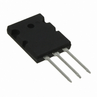
MOSFET N-CH 100V 170A TO-264
Manufacturer
IXYS
Series
PolarHT™r
Datasheet
1.IXTQ170N10P.pdf
(5 pages)
Specifications of IXTK170N10P
Fet Type
MOSFET N-Channel, Metal Oxide
Fet Feature
Standard
Rds On (max) @ Id, Vgs
9 mOhm @ 500mA, 10V
Drain To Source Voltage (vdss)
100V
Current - Continuous Drain (id) @ 25° C
170A
Vgs(th) (max) @ Id
5V @ 250µA
Gate Charge (qg) @ Vgs
198nC @ 10V
Input Capacitance (ciss) @ Vds
6000pF @ 25V
Power - Max
714W
Mounting Type
Through Hole
Package / Case
TO-264
Configuration
Single
Transistor Polarity
N-Channel
Resistance Drain-source Rds (on)
0.009 Ohms
Drain-source Breakdown Voltage
100 V
Gate-source Breakdown Voltage
+/- 20 V
Continuous Drain Current
170 A
Power Dissipation
714 W
Maximum Operating Temperature
+ 175 C
Mounting Style
Through Hole
Minimum Operating Temperature
- 55 C
Vdss, Max, (v)
100
Id(cont), Tc=25°c, (a)
170
Rds(on), Max, Tj=25°c, (?)
0.009
Ciss, Typ, (pf)
6000
Qg, Typ, (nc)
198
Trr, Typ, (ns)
120
Pd, (w)
715
Rthjc, Max, (k/w)
0.21
Package Style
TO-264
Lead Free Status / RoHS Status
Lead free / RoHS Compliant
Available stocks
Company
Part Number
Manufacturer
Quantity
Price
Company:

Part Number:
IXTK170N10P
Manufacturer:
IXYS
Quantity:
35 500


Symbol
(T
g
C
C
C
t
t
t
t
Q
Q
Q
R
R
Source-Drain Diode
Symbol
I
I
V
t
Q
Note 1. Pulse test, t ≤ 300μs, duty cycle, d ≤ 2%.
IXYS Reserves the Right to Change Limits, Test Conditions, and Dimensions.
IXYS MOSFETs and IGBTs are covered
by one or more of the following U.S. patents: 4,850,072
(T
S
SM
d(on)
r
d(off)
f
rr
TO-268 (IXTT) Outline
fs
SD
iss
oss
rss
thJC
thCS
g(on)
gs
gd
RM
J
J
= 25°C, Unless Otherwise Specified)
= 25°C, Unless Otherwise Specified)
(TO-264)
V
V
Resistive Switching Times
V
R
V
(TO-3P)
Test Conditions
V
Repetitive, Pulse Width Limited by T
I
I
V
Test Conditions
F
F
DS
GS
GS
GS
GS
R
G
= I
= 25A, -di/dt = 100A/μs,
= 50V, V
= 10V, V
= 3.3Ω (External)
= 0V
= 10V, I
= 0V, V
= 10V, V
S
, V
GS
= 0V, Note 1
GS
DS
D
DS
DS
= 0V
= 0.5 • I
= 25V, f = 1MHz
= 0.5 • V
= 0.5 • V
4,835,592
4,881,106
D25
DSS
, Note 1
DSS
4,931,844
5,017,508
5,034,796
, I
, I
D
D
= 60A
= 0.5 • I
5,049,961
5,063,307
5,187,117
JM
D25
5,237,481
5,381,025
5,486,715
Characteristic Values
Min.
Min.
Characteristic Values
50
6,162,665
6,259,123 B1
6,306,728 B1
6000
2340
Typ.
0.25
0.15
120
Typ.
730
198
107
2.0
35
50
90
33
39
72
0.21 °C/W
Max.
6,404,065 B1
6,534,343
6,583,505
Max.
170
350
1.5
°C/W
°C/W
μC
nC
nC
nC
pF
pF
pF
ns
ns
ns
ns
ns
IXTT170N10P IXTQ170N10P
S
A
A
V
6,683,344
6,710,405 B2 6,759,692
6,710,463
TO-264 AA ( IXTK) Outline
TO-3P (IXTQ) Outline
6,727,585
6,771,478 B2 7,071,537
Dim.
A
A1
A2
b
b1
b2
c
D
E
e
J
K
L
L1
P
Q
Q1
R
R1
S
T
25.91
19.81
20.32
4.82
2.54
2.00
1.12
2.39
2.90
0.53
0.00
0.00
2.29
3.17
6.07
8.38
3.81
1.78
6.04
1.57
Min.
Millimeter
5.46 BSC
IXTK170N10P
7,005,734 B2
7,063,975 B2
26.16
19.96
20.83
Max.
5.13
2.89
2.10
1.42
2.69
3.09
0.83
0.25
0.25
2.59
3.66
6.27
8.69
4.32
2.29
6.30
1.83
Back Side
1.020
Min.
.190
.100
.079
.044
.094
.114
.021
.780
.000
.000
.800
.090
.125
.239
.330
.150
.070
.238
.062
.215 BSC
Inches
7,157,338B2
Max.
1.030
.202
.114
.083
.056
.106
.122
.033
.786
.010
.010
.820
.102
.144
.247
.342
.170
.090
.248
.072
1 = Gate
2 = Drain
3 = Source
Tab = Drain
Related parts for IXTK170N10P
Image
Part Number
Description
Manufacturer
Datasheet
Request
R


Part Number:
Description:
HiPerFET Power MOSFETs
Manufacturer:
IXYS Corporation
Datasheet:
Part Number:
Description:
J-K-Type Flip-Flop
Manufacturer:
IXYS Corporation
Datasheet:
Part Number:
Description:
HiPerRF Power MOSFETs
Manufacturer:
IXYS Corporation
Datasheet:
Part Number:
Description:
Rectifier Module for Three Phase Power Factor Correction
Manufacturer:
IXYS Corporation
Datasheet:
Part Number:
Description:
Thyristor Modules Thyristor/Diode Modules
Manufacturer:
IXYS Corporation
Datasheet:
Part Number:
Description:
Thyristor Modules Thyristor/Diode Modules
Manufacturer:
IXYS Corporation
Datasheet:
Part Number:
Description:
Thyristor Modules Thyristor/Diode Modules
Manufacturer:
IXYS Corporation
Datasheet:
Part Number:
Description:
Thyristor Modules Thyristor/Diode Modules
Manufacturer:
IXYS Corporation
Datasheet:
Part Number:
Description:
Thyristor Modules /Diode Modules
Manufacturer:
IXYS Corporation
Datasheet:
Part Number:
Description:
Thyristor Modules /Diode Modules
Manufacturer:
IXYS Corporation
Datasheet:
Part Number:
Description:
Thyristor Modules Thyristor/Diode Modules
Manufacturer:
IXYS Corporation
Datasheet: