IXFX66N50Q2 IXYS, IXFX66N50Q2 Datasheet - Page 2
IXFX66N50Q2
Manufacturer Part Number
IXFX66N50Q2
Description
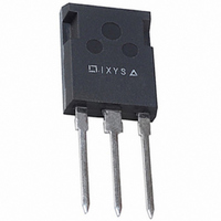
MOSFET N-CH 500V 66A PLUS247
Manufacturer
IXYS
Series
HiPerFET™r
Datasheet
1.IXFX66N50Q2.pdf
(5 pages)
Specifications of IXFX66N50Q2
Fet Type
MOSFET N-Channel, Metal Oxide
Fet Feature
Standard
Rds On (max) @ Id, Vgs
80 mOhm @ 500mA, 10V
Drain To Source Voltage (vdss)
500V
Current - Continuous Drain (id) @ 25° C
66A
Vgs(th) (max) @ Id
5.5V @ 8mA
Gate Charge (qg) @ Vgs
200nC @ 10V
Input Capacitance (ciss) @ Vds
9125pF @ 25V
Power - Max
735W
Mounting Type
Through Hole
Package / Case
PLUS247™-3
Configuration
Single
Transistor Polarity
N-Channel
Resistance Drain-source Rds (on)
0.074 Ohms
Drain-source Breakdown Voltage
500 V
Gate-source Breakdown Voltage
+/- 30 V
Continuous Drain Current
66 A
Power Dissipation
735 W
Maximum Operating Temperature
+ 150 C
Mounting Style
Through Hole
Minimum Operating Temperature
- 55 C
Vdss, Max, (v)
500
Id(cont), Tc=25°c, (a)
66
Rds(on), Max, Tj=25°c, (?)
0.08
Ciss, Typ, (pf)
9125
Qg, Typ, (nc)
200
Trr, Typ, (ns)
-
Trr, Max, (ns)
250
Pd, (w)
735
Rthjc, Max, (ºc/w)
0.17
Package Style
PLUS247
Lead Free Status / RoHS Status
Lead free / RoHS Compliant


IXYS reserves the right to change limits, test conditions, and dimensions.
Source-Drain Diode
Symbol
I
I
V
t
Q
I
IXYS MOSFETs and IGBTs are covered by
Symbol
g
C
C
C
t
t
t
t
Q
Q
Q
R
R
one or moreof the following U.S. patents:
SM
RM
S
rr
d(on)
d(off)
f
r
SD
fs
RM
thJC
thCK
iss
oss
rss
g(on)
gs
gd
Test Conditions
V
Repetitive; pulse width limited by T
I
Pulse test, t ≤ 300 µs, duty cycle d ≤ 2 %
F
GS
Test Conditions
V
TO-264
= I
I
DS
F
= 0 V
S
= 25A, -di/dt = 100 A/µs, V
, V
= 10 V; I
V
V
R
V
GS
GS
GS
GS
G
= 1.0 Ω (External),
= 0 V,
= 0 V, V
= 10 V, V
= 10 V, V
D
= 0.5 • I
4,835,592
4,850,072
4,881,106
DS
DS
DS
= 25 V, f = 1 MHz
= 0.5 • V
= 0.5 • V
D25
4,931,844
5,017,508
5,034,796
, pulse test
(T
(T
R
DSS
DSS
J
= 100 V
J
= 25°C, unless otherwise specified)
= 25°C, unless otherwise specified)
, I
, I
5,049,961
5,063,307
5,187,117
JM
D
D
= 0.5 • I
= 0.5 • I
min.
5,237,481
5,381,025
5,486,715
D25
D25
min.
Characteristic Values
30
Characteristic Values
8400
1290
typ.
0.15
typ.
310
200
10
6,162,665
6,259,123 B1
6,306,728 B1
44
32
16
60
10
47
98
1
0.17
max.
max.
264
250
1.5
66
6,404,065 B1
6,534,343
6,583,505
K/W
K/W
µC
nC
nC
nC
ns
pF
pF
pF
ns
ns
ns
ns
A
A
A
V
S
TO-264 AA Outline
PLUS 247
6,683,344
6,710,405B2
6,710,463
Terminals: 1 - Gate
Dim.
A
A1
A2
b
b1
b2
c
D
E
e
J
K
L
L1
P
Q
Q1
R
R1
S
T
Dim.
A
A
A
b
b
b
C
D
E
e
L
L1
Q
R
1
2
1
2
IXFK 66N50Q2
IXFX 66N50Q2
25.91
19.81
20.32
Min.
4.82
2.54
2.00
1.12
2.39
2.90
0.53
0.00
0.00
2.29
3.17
6.07
8.38
3.81
1.78
6.04
1.57
20.80
15.75
19.81
TM
Millimeter
Min.
4.83
2.29
1.91
1.14
1.91
2.92
0.61
3.81
5.59
4.32
5.46 BSC
6,727,585
6,759,692
Millimeter
5.45 BSC
Outline
2 - Drain (Collector)
3 - Source (Emitter)
4 - Drain (Collector)
26.16
19.96
20.83
Max.
5.13
2.89
2.10
1.42
2.69
3.09
0.83
0.25
0.25
2.59
3.66
6.27
8.69
4.32
2.29
6.30
1.83
21.34
16.13
20.32
Max.
5.21
2.54
2.16
1.40
2.13
3.12
0.80
4.32
6.20
4.83
Min.
1.020
.190
.100
.079
.044
.094
.114
.021
.780
.000
.000
.800
.090
.125
.239
.330
.150
.070
.238
.062
.215 BSC
Min. Max.
.190
.090
.075
.045
.075
.115
.024
.819
.620
.780
.150
.220 0.244
.170
Inches
.215 BSC
Inches
Max.
1.030
.202
.114
.083
.056
.106
.122
.033
.786
.010
.010
.820
.102
.144
.247
.342
.170
.090
.248
.072
.205
.100
.085
.055
.084
.123
.031
.840
.635
.800
.170
.190
Related parts for IXFX66N50Q2
Image
Part Number
Description
Manufacturer
Datasheet
Request
R


Part Number:
Description:
HiPerFET Power MOSFETs
Manufacturer:
IXYS Corporation
Datasheet:
Part Number:
Description:
J-K-Type Flip-Flop
Manufacturer:
IXYS Corporation
Datasheet:
Part Number:
Description:
HiPerRF Power MOSFETs
Manufacturer:
IXYS Corporation
Datasheet:
Part Number:
Description:
Rectifier Module for Three Phase Power Factor Correction
Manufacturer:
IXYS Corporation
Datasheet:
Part Number:
Description:
Thyristor Modules Thyristor/Diode Modules
Manufacturer:
IXYS Corporation
Datasheet:
Part Number:
Description:
Thyristor Modules Thyristor/Diode Modules
Manufacturer:
IXYS Corporation
Datasheet:
Part Number:
Description:
Thyristor Modules Thyristor/Diode Modules
Manufacturer:
IXYS Corporation
Datasheet:
Part Number:
Description:
Thyristor Modules Thyristor/Diode Modules
Manufacturer:
IXYS Corporation
Datasheet:
Part Number:
Description:
Thyristor Modules /Diode Modules
Manufacturer:
IXYS Corporation
Datasheet:
Part Number:
Description:
Thyristor Modules /Diode Modules
Manufacturer:
IXYS Corporation
Datasheet:
Part Number:
Description:
Thyristor Modules Thyristor/Diode Modules
Manufacturer:
IXYS Corporation
Datasheet: