STW77N65M5 STMicroelectronics, STW77N65M5 Datasheet
STW77N65M5
Specifications of STW77N65M5
STW77N65M5
Available stocks


Related parts for STW77N65M5


STW77N65M5 Summary of contents
Page 1
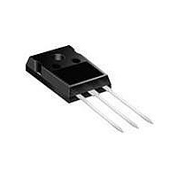
... Power MOSFETs, making it especially suited for applications which require superior power density and outstanding efficiencies. Table 1. Device summary Order codes STW77N65M5 July 2009 max I DS(on) D < 0.038 Ω Figure 1. Marking 77N65M5 Doc ID 15322 Rev 2 STW77N65M5 TO-247 Internal schematic diagram Package Packaging TO-247 Tube TO-247 1/13 www.st.com 13 ...
Page 2
... Contents Contents 1 Electrical ratings . . . . . . . . . . . . . . . . . . . . . . . . . . . . . . . . . . . . . . . . . . . . 3 2 Electrical characteristics . . . . . . . . . . . . . . . . . . . . . . . . . . . . . . . . . . . . . 4 2.1 Electrical characteristics (curves) 3 Test circuits 4 Package mechanical data . . . . . . . . . . . . . . . . . . . . . . . . . . . . . . . . . . . . 10 5 Revision history . . . . . . . . . . . . . . . . . . . . . . . . . . . . . . . . . . . . . . . . . . . 13 2/ Doc ID 15322 Rev 2 STW77N65M5 . . . . . . . . . . . . . . . . . . . . . . . . . . . . 5 ...
Page 3
... STW77N65M5 1 Electrical ratings Table 2. Absolute maximum ratings Symbol V Gate- source voltage GS I Drain current (continuous Drain current (continuous (1) I Drain current (pulsed Total dissipation at T TOT Max current during repetitive or single pulse avalanche I AR (pulse width limited by T Single pulse avalanche energy ...
Page 4
... D Parameter Test conditions V = 100 MHz 520 520 MHz open drain V = 520 Figure 16) (see DSS DSS Doc ID 15322 Rev 2 STW77N65M5 Min. Typ 650 =125 ° 250 µ 34.5 A 0.030 Min. Typ. 9800 - 200 6 - 590 - 1000 - 1.2 = 34.5 A, 200 - 60 70 Max. Unit V 1 µA 100 µ ...
Page 5
... STW77N65M5 Table 6. Switching times Symbol t Turn-on delay time d(on) t Rise time r t Turn-off-delay time d(off) t Fall time f Table 7. Source drain diode Symbol I Source-drain current SD (1) I Source-drain current (pulsed) SDM (2) V Forward on voltage SD t Reverse recovery time rr Q Reverse recovery charge rr I Reverse recovery current ...
Page 6
... Figure 5. AM04965v1 (V) DS AM04969v1 R DS(on 0.041 480 400 0.036 0.031 320 240 0.026 160 0.021 0.016 80 0 0.011 150 200 Q (nC) g Doc ID 15322 Rev 2 STW77N65M5 Thermal impedance Transfer characteristics I D (A) V =2V DS 140 120 100 Static drain-source on resistance (Ω) I =34. =10V ...
Page 7
... STW77N65M5 Figure 8. Capacitance variations C (pF) 100000 10000 1000 100 Figure 10. Normalized gate threshold voltage vs temperature V GS(th) (norm) 1.10 1.00 0.90 0.80 0.70 -50 - Figure 12. Source-drain diode forward characteristics V SD (V) T =-50°C J 1.2 1.0 0.8 0.6 T =150°C J 0.4 0 Figure 9. AM04970v1 E oss (µ ...
Page 8
... Electrical characteristics Figure 14. Switching losses vs gate resistance (1) E (µJ) I =25A D 600 V =400V DD L=50µH 500 400 300 200 100 Eon including reverse recovery of a SiC diode 8/13 AM04973v1 Eon Eoff (Ω) G Doc ID 15322 Rev 2 STW77N65M5 ...
Page 9
... STW77N65M5 3 Test circuits Figure 15. Switching times test circuit for resistive load D.U. Figure 17. Test circuit for inductive load switching and diode recovery times FAST L=100µH G D.U.T. DIODE Ω Figure 19. Unclamped inductive waveform Figure 16. Gate charge test circuit 3.3 2200 µF µ ...
Page 10
... Package mechanical data 4 Package mechanical data In order to meet environmental requirements, ST offers these devices in different grades of ® ECOPACK packages, depending on their level of environmental compliance. ECOPACK specifications, grade definitions and product status are available at: www.st.com. ECOPACK trademark. 10/13 Doc ID 15322 Rev 2 STW77N65M5 ® ...
Page 11
... STW77N65M5 Dim øP øR S TO-247 Mechanical data mm. Min. Typ 4.85 2.20 1.0 2.0 3.0 0.40 19.85 15.45 5.45 14.20 3.70 18.50 3.55 4.50 5.50 Doc ID 15322 Rev 2 Package mechanical data Max. 5.15 2.60 1.40 2.40 3.40 0.80 20.15 15.75 14.80 4.30 3 ...
Page 12
... Revision history 5 Revision history Table 8. Document revision history Date 20-Jan-2009 14-Jul-2009 12/13 Revision 1 First release. 2 Document status promoted from preliminary data to datasheet. Doc ID 15322 Rev 2 STW77N65M5 Changes ...
Page 13
... STW77N65M5 Information in this document is provided solely in connection with ST products. STMicroelectronics NV and its subsidiaries (“ST”) reserve the right to make changes, corrections, modifications or improvements, to this document, and the products and services described herein at any time, without notice. All ST products are sold pursuant to ST’s terms and conditions of sale. ...