IXFX90N30 IXYS, IXFX90N30 Datasheet
首页 Discrete Semiconductor Products MOSFETs, GaNFETs - Single IXFX90N30
Manufacturer Part Number
IXFX90N30
Description
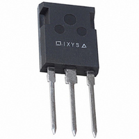
MOSFET N-CH 300V 90A PLUS247
Specifications of IXFX90N30
Fet Type
MOSFET N-Channel, Metal Oxide
Fet Feature
Standard
Rds On (max) @ Id, Vgs
33 mOhm @ 500mA, 10V
Drain To Source Voltage (vdss)
300V
Current - Continuous Drain (id) @ 25° C
90A
Vgs(th) (max) @ Id
4V @ 8mA
Gate Charge (qg) @ Vgs
360nC @ 10V
Input Capacitance (ciss) @ Vds
10000pF @ 25V
Power - Max
560W
Mounting Type
Through Hole
Package / Case
PLUS247™-3
Configuration
Single
Transistor Polarity
N-Channel
Resistance Drain-source Rds (on)
0.033 Ohms
Forward Transconductance Gfs (max / Min)
70 s
Drain-source Breakdown Voltage
300 V
Gate-source Breakdown Voltage
+/- 20 V
Continuous Drain Current
90 A
Power Dissipation
560 W
Maximum Operating Temperature
+ 150 C
Mounting Style
Through Hole
Minimum Operating Temperature
- 55 C
Vdss, Max, (v)
300
Id(cont), Tc=25°c, (a)
90
Rds(on), Max, Tj=25°c, (?)
0.033
Ciss, Typ, (pf)
10000
Qg, Typ, (nc)
360
Trr, Typ, (ns)
-
Trr, Max, (ns)
250
Pd, (w)
568
Rthjc, Max, (ºc/w)
0.22
Package Style
PLUS247
Lead Free Status / RoHS Status
Lead free / RoHS Compliant
Available stocks
HiPerFET
Power MOSFETs
Single MOSFET Die
Symbol
V
V
V
V
I
I
I
I
E
E
dv/dt
P
T
T
T
T
M
Weight
Symbol
V
V
I
I
R
© 2001 IXYS All rights reserved
DM
D25
D104
AR
GSS
DSS
J
JM
stg
L
DGR
GS
GSM
AR
AS
D
DSS
GS(th)
DSS
DS(on)
d
Test Conditions
Test Conditions
V
V
S
GS
DS
GS
GS
J
J
C
C
C
C
C
C
J
C
GS
DS
= V
= 0 V, I
DM
GS
DSS
, I
TM
D
D
= 3mA
= 8mA
D
DS
G
D25
GS
DD
J
J
J
DSS
JM
IXFK 90N30
IXFX 90N30
300
min.
2.0
Characteristic Values
Maximum Ratings
typ.
max.
4.0 V
V
PLUS 247
TO-264 AA (IXFK)
G = Gate
S = Source
Features
l
l
l
l
l
l
Applications
l
l
l
l
l
l
Advantages
l
l
l
V
I
R
t
D25
rr
DSS
DS(on)
DS (on)
G
TM
250 ns
D
TM
G
D
= 300
=
=
S
D = Drain
TAB = Drain
TM
90
33 m
98537A (12/01)
V
A
(TAB)
(TAB)
Related parts for IXFX90N30
IXFX90N30 Summary of contents
... Weight Symbol Test Conditions 3mA DSS 8mA GS(th GSS DSS DS DSS GS R DS(on D25 © 2001 IXYS All rights reserved IXFX 90N30 IXFK 90N30 Maximum Ratings DSS Characteristic Values J min. typ. max. 300 2 300 DSS D25 = DS(on) t 250 ns rr PLUS 247 TM ...
... R thJC R thCK Source-Drain Diode Symbol Test Conditions IXYS reserves the right to change limits, test conditions, and dimensions. Characteristic Values J min. typ. max. DSS D D25 DSS D D25 Characteristic Values J min. typ. max IXFK 90N30 IXFX 90N30 TM PLUS 247 Outline Dim. Millimeter Inches Min ...
... I - Amperes D Fig.3 R vs. Drain Current DS(on) 100 150 -50 - Degrees C C Fig.5 Drain Current vs. Case Temperature © 2001 IXYS All rights reserved 150 7V 125 6V 100 25° 160 200 160 140 120 100 100 125 150 IXFK 90N30 IXFX 90N30 ...
... 0.2 0.4 0.6 0 Volts SD Fig.9 Drain Current vs Drain to Source Voltage 1.000 0.100 0.010 0.001 - Fig.10 Transient Thermal Impedance IXYS reserves the right to change limits, test conditions, and dimensions 0.5 200 250 300 1.0 1.2 1 Pulse Width - Seconds IXFK 90N30 IXFX 90N30 ...
Related keywords
ixfx90n30 IXFX90N30 datasheet IXFX90N30 data sheet IXFX90N30 pdf datasheet IXFX90N30 component IXFX90N30 part IXFX90N30 distributor IXFX90N30 RoHS IXFX90N30 datasheet download