NTB5412NT4G ON Semiconductor, NTB5412NT4G Datasheet

MOSFET N-CH 60V 60A D2PAK

NTB5412NT4G

Manufacturer Part Number
NTB5412NT4G
Description
MOSFET N-CH 60V 60A D2PAK
Manufacturer
ON Semiconductor
Datasheet

Specifications of NTB5412NT4G

Fet Type
MOSFET N-Channel, Metal Oxide
Fet Feature
Standard
Rds On (max) @ Id, Vgs
14 mOhm @ 30A, 10V
Drain To Source Voltage (vdss)
60V
Current - Continuous Drain (id) @ 25° C
60A
Vgs(th) (max) @ Id
4V @ 250µA
Gate Charge (qg) @ Vgs
85nC @ 0V
Input Capacitance (ciss) @ Vds
3220pF @ 25V
Power - Max
125W
Mounting Type
Surface Mount
Package / Case
D²Pak, TO-263 (2 leads + tab)
Configuration
Single
Transistor Polarity
N-Channel
Resistance Drain-source Rds (on)
11.1 Ohms
Forward Transconductance Gfs (max / Min)
58 S
Drain-source Breakdown Voltage
60 V
Gate-source Breakdown Voltage
+/- 20 V
Continuous Drain Current
60 A
Power Dissipation
125 W
Maximum Operating Temperature
+ 175 C
Mounting Style
SMD/SMT
Minimum Operating Temperature
- 55 C
Lead Free Status / RoHS Status
Contains lead / RoHS non-compliant

Available stocks

Company
Part Number
Manufacturer
Quantity
Price
Part Number:
NTB5412NT4G
Manufacturer:
ON Semiconductor
Quantity:
78
Part Number:
NTB5412NT4G
Manufacturer:
ON
Quantity:
12 500
NTB5412N, NTP5412N
Power MOSFET
60 Amps, 60 Volts
N-Channel D
Features
Applications
Stresses exceeding Maximum Ratings may damage the device. Maximum
Ratings are stress ratings only. Functional operation above the Recommended
Operating Conditions is not implied. Extended exposure to stresses above the
Recommended Operating Conditions may affect device reliability.
1. Surface mounted on FR4 board using 1 sq in pad size,
© Semiconductor Components Industries, LLC, 2008
November, 2008 − Rev. 1
MAXIMUM RATINGS
THERMAL RESISTANCE RATINGS
Drain−to−Source Voltage
Gate−to−Source Voltage − Continuous
Gate−to−Source Voltage − Nonrepetitive
(T
Continuous Drain
Current R
(Note 1)
Power Dissipation
R
Pulsed Drain Current
Operating and Storage Temperature Range
Source Current (Body Diode)
Single Pulse Drain−to−Source Avalanche
Energy − Starting T
(V
L = 0.1 mH, R
Lead Temperature for Soldering
Purposes, 1/8″ from Case for 10 Seconds
Junction−to−Case (Drain) Steady State
(Note 1)
Low R
High Current Capability
Avalanche Energy Specified
These are Pb−Free Devices
LED Lighting and LED Backlight Drivers
DC−DC Converters
DC Motor Drivers
Power Supplies Secondary Side Synchronous Rectification
qJC
(Cu Area 1.127 sq in [1 oz] including traces).
P
DD
< 10 ms)
= 50 V
(Note 1)
DS(on)
qJC
dc
, V
G
= 25 W)
GS
Parameter
Parameter
J
= 10 V
= 25°C
Steady
Steady
(T
State
State
dc
J
= 25°C Unless otherwise specified)
, I
t
L(pk)
p
= 10 ms
2
T
T
T
= 60 A,
C
PAK, TO-220
C
C
= 100°C
= 25°C
= 25°C
Symbol
Symbol
T
V
R
R
J
V
V
E
I
P
DSS
, T
T
I
DM
I
qJC
qJA
GS
GS
AS
D
S
D
L
stg
−55 to
Value
$20
$30
Max
43.2
125
155
175
180
260
1.2
60
60
44
60
1
°C/W
Unit
Unit
mJ
°C
°C
W
V
V
V
A
A
A
See detailed ordering and shipping information in the package
dimensions section on page 5 of this data sheet.
Gate
V
1
(BR)DSS
1
60 V
2
3
5412NG
AYWW
Drain
Drain
NTP
4
ORDERING INFORMATION
2
G
4
MARKING DIAGRAM
& PIN ASSIGNMENT
CASE 221A
TO−220AB
http://onsemi.com
STYLE 5
3
Source
R
14 mW @ 10 V
DS(ON)
N−Channel
G
A
Y
WW
D
Publication Order Number:
MAX
Gate
= Pb−Free Device
= Assembly Location
= Year
= Work Week
S
1
1
5412NG
AYWW
Drain
CASE 418B
Drain
2
NTB
STYLE 2
4
2
3
D
NTB5412N/D
(Note 1)
2
I
D
PAK
60 A
MAX
3
Source
4

Related parts for NTB5412NT4G

NTB5412NT4G Summary of contents

Page 1

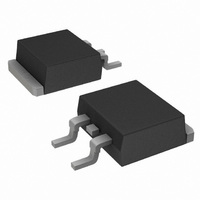
NTB5412N, NTP5412N Power MOSFET 60 Amps, 60 Volts 2 N-Channel D PAK, TO-220 Features • Low R DS(on) • High Current Capability • Avalanche Energy Specified • These are Pb−Free Devices Applications • LED Lighting and LED Backlight Drivers • ...

Page 2

ELECTRICAL CHARACTERISTICS Characteristics OFF CHARACTERISTICS Drain−to−Source Breakdown Voltage Drain−to−Source Breakdown Voltage Temper- ature Coefficient Zero Gate Voltage Drain Current Gate−Body Leakage Current ON CHARACTERISTICS (Note 2) Gate Threshold Voltage Negative Threshold Temperature Coefficient Drain−to−Source On Voltage Static Drain−to−Source On−Resistance Forward ...

Page 3

V 100 DRAIN−TO−SOURCE VOLTAGE (V) DS Figure 1. On−Region Characteristics 0.050 0.045 0.040 0.035 0.030 0.025 0.020 0.015 0.010 0.005 GATE−TO−SOURCE VOLTAGE ...

Page 4

C rss DRAIN−TO−SOURCE VOLTAGE (V) DS Figure 7. Capacitance Variation 1000 ...

Page 5

... ORDERING INFORMATION Device NTP5412NG NTB5412NT4G †For information on tape and reel specifications, including part orientation and tape sizes, please refer to our Tape and Reel Packaging Specifications Brochure, BRD8011/D. TYPICAL PERFORMANCE CURVES Surface−Mounted on FR4 Board using pad size 0.001 ...

Page 6

... SEATING PLANE 0.13 (0.005 VARIABLE CONFIGURATION ZONE VIEW W−W VIEW W−W 1 *For additional information on our Pb−Free strategy and soldering details, please download the ON Semiconductor Soldering and Mounting Techniques Reference Manual, SOLDERRM/D. PACKAGE DIMENSIONS 2 D PAK 3 CASE 418B−04 ISSUE ...

Page 7

... Opportunity/Affirmative Action Employer. This literature is subject to all applicable copyright laws and is not for resale in any manner. PUBLICATION ORDERING INFORMATION LITERATURE FULFILLMENT: Literature Distribution Center for ON Semiconductor P.O. Box 5163, Denver, Colorado 80217 USA Phone: 303−675−2175 or 800−344−3860 Toll Free USA/Canada Fax: 303− ...

Related keywords