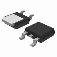
NTD25P03LG ON Semiconductor, NTD25P03LG Datasheet - Page 6

NTD25P03LG
Manufacturer Part Number
NTD25P03LG
Description
MOSFET P-CH 30V 25A DPAK
Manufacturer
ON Semiconductor
Type
Power MOSFETr
Datasheet
1.NTD25P03LT4G.pdf
(9 pages)
Specifications of NTD25P03LG
Fet Type
MOSFET P-Channel, Metal Oxide
Fet Feature
Logic Level Gate
Rds On (max) @ Id, Vgs
80 mOhm @ 25A, 5V
Drain To Source Voltage (vdss)
30V
Current - Continuous Drain (id) @ 25° C
25A
Vgs(th) (max) @ Id
2V @ 250µA
Gate Charge (qg) @ Vgs
20nC @ 5V
Input Capacitance (ciss) @ Vds
1260pF @ 25V
Power - Max
75W
Mounting Type
Surface Mount
Package / Case
DPak, TO-252 (2 leads+tab), SC-63
Configuration
Single
Transistor Polarity
P-Channel
Resistance Drain-source Rds (on)
0.08 Ohm @ 5 V
Forward Transconductance Gfs (max / Min)
13 S
Drain-source Breakdown Voltage
30 V
Gate-source Breakdown Voltage
+/- 15 V
Continuous Drain Current
25 A
Power Dissipation
75000 mW
Maximum Operating Temperature
+ 150 C
Mounting Style
SMD/SMT
Minimum Operating Temperature
- 55 C
Number Of Elements
1
Polarity
P
Channel Mode
Enhancement
Drain-source On-res
0.08Ohm
Drain-source On-volt
30V
Gate-source Voltage (max)
±15V
Operating Temp Range
-55C to 150C
Operating Temperature Classification
Military
Mounting
Surface Mount
Pin Count
2 +Tab
Package Type
DPAK
Lead Free Status / RoHS Status
Lead free / RoHS Compliant
Other names
NTD25P03LG
NTD25P03LGOS
NTD25P03LGOS
Available stocks
Company
Part Number
Manufacturer
Quantity
Price
Company:
Part Number:
NTD25P03LG
Manufacturer:
ON
Quantity:
5 025
Company:
Part Number:
NTD25P03LG
Manufacturer:
ON
Quantity:
12 500
Company:
Part Number:
NTD25P03LG
Manufacturer:
ON
Quantity:
12 500
the maximum simultaneous drain−to−source voltage and
drain current that a transistor can handle safely when it is
forward biased. Curves are based upon maximum peak
junction temperature and a case temperature (T
Peak repetitive pulsed power limits are determined by using
the thermal response data in conjunction with the procedures
discussed in AN569, “Transient Thermal Resistance −
General Data and Its Use.”
traverse any load line provided neither rated peak current
(I
transition time (t
total power averaged over a complete switching cycle must
not exceed (T
in switching circuits with unclamped inductive loads. For
DM
The Forward Biased Safe Operating Area curves define
Switching between the off−state and the on−state may
A power MOSFET designated E−FET can be safely used
100
0.1
10
) nor rated voltage (V
1
0.1
V
SINGLE PULSE
T
C
Figure 11. Maximum Rated Forward Biased
GS
−V
= 25°C
= −20 V
J(MAX)
DS
, DRAIN−TO−SOURCE VOLTAGE (VOLTS)
r
, t
f
R
THERMAL LIMIT
PACKAGE LIMIT
) does not exceed 10 ms. In addition the
DS(on)
− T
Safe Operating Area
1
C
)/(R
LIMIT
DSS
qJC
) is exceeded, and that the
).
10
SAFE OPERATING AREA
C
) of 25°C.
10 ms
100 ms
1 ms
dc
http://onsemi.com
100
6
reliable operation, the stored energy from circuit inductance
dissipated in the transistor while in avalanche must be less
than the rated limit and must be adjusted for operating
conditions differing from those specified. Although industry
practice is to rate in terms of energy, avalanche energy
capability is not a constant. The energy rating decreases
non−linearly with an increase of peak current in avalanche
and peak junction temperature.
drain−to−source avalanche at currents up to rated pulsed
current (I
continuous current (I
custom. The energy rating must be derated for temperature
as shown in the accompanying graph (Figure 12). Maximum
energy at currents below rated continuous I
assumed to equal the values indicated.
200
180
160
140
120
100
80
60
40
20
Although many E−FETs can withstand the stress of
0
25
Figure 12. Maximum Avalanche Energy versus
T
DM
J
, STARTING JUNCTION TEMPERATURE (°C)
), the energy rating is specified at rated
50
Starting Junction Temperature
D
), in accordance with industry
75
100
D
I
125
D
can safely be
= −20 A
150


