IRF630S Vishay, IRF630S Datasheet - Page 2
IRF630S
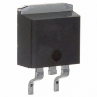
Manufacturer Part Number
IRF630S
Description
MOSFET N-CH 200V 9A D2PAK
Manufacturer
Vishay
Specifications of IRF630S
Fet Type
MOSFET N-Channel, Metal Oxide
Fet Feature
Standard
Rds On (max) @ Id, Vgs
400 mOhm @ 5.4A, 10V
Drain To Source Voltage (vdss)
200V
Current - Continuous Drain (id) @ 25° C
9A
Vgs(th) (max) @ Id
4V @ 250µA
Gate Charge (qg) @ Vgs
43nC @ 10V
Input Capacitance (ciss) @ Vds
800pF @ 25V
Power - Max
3W
Mounting Type
Surface Mount
Package / Case
D²Pak, TO-263 (2 leads + tab)
Lead Free Status / RoHS Status
Contains lead / RoHS non-compliant
Available stocks
Company
Part Number
Manufacturer
Quantity
Price
Company:

Part Number:
IRF630S
Manufacturer:
IR
Quantity:
32 050
Company:
Part Number:
IRF630STRR
Manufacturer:
IR
Quantity:
32 000
Part Number:
IRF630STRR
Manufacturer:
VISHAY/威世
Quantity:
20 000


Source-Drain Ratings and Characteristics
Thermal Resistance
IRF630N/S/L
Electrical Characteristics @ T
www.irf.com
R
R
R
R
V
∆V
R
V
g
I
I
Q
Q
Q
t
t
t
t
C
C
C
I
I
V
t
Q
t
L
L
DSS
GSS
S
SM
rr
on
d(on)
r
d(off)
f
fs
D
S
θJC
θCS
θJA
θJA
SD
(BR)DSS
GS(th)
DS(on)
g
gs
gd
iss
oss
rss
rr
(BR)DSS
/∆T
J
Drain-to-Source Leakage Current
Continuous Source Current
(Body Diode)
Pulsed Source Current
(Body Diode)
Diode Forward Voltage
Reverse Recovery Time
Reverse Recovery Charge
Forward Turn-On Time
Drain-to-Source Breakdown Voltage
Breakdown Voltage Temp. Coefficient
Static Drain-to-Source On-Resistance
Gate Threshold Voltage
Forward Transconductance
Gate-to-Source Forward Leakage
Gate-to-Source Reverse Leakage
Total Gate Charge
Gate-to-Source Charge
Gate-to-Drain ("Miller") Charge
Turn-On Delay Time
Rise Time
Turn-Off Delay Time
Fall Time
Input Capacitance
Output Capacitance
Reverse Transfer Capacitance
Internal Drain Inductance
Internal Source Inductance
Junction-to-Case
Case-to-Sink, Flat, Greased Surface
Junction-to-Ambient
Junction-to-Ambient (PCB mount)
Parameter
Parameter
Parameter
„
J
= 25°C (unless otherwise specified)
…
200
–––
–––
–––
–––
–––
–––
–––
–––
–––
–––
–––
–––
–––
–––
–––
–––
–––
Min. Typ. Max. Units
Min. Typ. Max. Units
2.0
4.9
–––
–––
–––
–––
–––
–––
„
Intrinsic turn-on time is negligible (turn-on is dominated by L
0.26
–––
––– 0.30
–––
–––
–––
–––
–––
––– -100
–––
–––
–––
575
–––
–––
–––
117
542
7.9
4.5
7.5
14
27
15
89
25
–––
–––
–––
–––
250
100
–––
–––
–––
–––
–––
–––
–––
–––
176
813
4.0
6.5
1.3
9.3
25
35
17
37
V/°C
µA
nA
nC
ns
nC
pF
nH
ns
Ω
V
V
V
S
Typ.
0.50
–––
–––
–––
V
Reference to 25°C, I
V
V
V
V
V
V
V
I
V
V
V
I
R
R
Between lead,
6mm (0.25in.)
from package
and center of die contact
V
V
ƒ = 1.0MHz
MOSFET symbol
showing the
integral reverse
p-n junction diode.
T
T
di/dt = 100A/µs
D
D
J
J
GS
GS
DS
DS
DS
DS
GS
GS
DS
GS
DD
GS
DS
G
D
= 5.4A
= 5.4A
= 25°C, I
= 25°C, I
= 18Ω
= 13Ω
= 0V, I
= 10V, I
= V
= 50V, I
= 200V, V
= 160V, V
= 20V
= -20V
= 160V
= 10V
= 100V
= 0V
= 25V
GS
, I
D
ƒ
S
F
ƒ
D
D
D
Conditions
= 250µA
Conditions
= 5.4A, V
= 5.4A
= 5.4A
= 250µA
= 5.4A ƒ
GS
GS
Max.
ƒ
1.83
–––
62
40
= 0V
= 0V, T
D
= 1mA
GS
ƒ
J
G
= 0V
= 150°C
G
Units
S
°C/W
+L
ƒ
D
D
S
)
S
D
2
Related parts for IRF630S
Image
Part Number
Description
Manufacturer
Datasheet
Request
R

Part Number:
Description:
357-036-542-201 CARDEDGE 36POS DL .156 BLK LOPRO
Manufacturer:
Vishay
Datasheet:
Part Number:
Description:
357-036-542-201 CARDEDGE 36POS DL .156 BLK LOPRO
Manufacturer:
Vishay
Datasheet:
Part Number:
Description:
357-036-542-201 CARDEDGE 36POS DL .156 BLK LOPRO
Manufacturer:
Vishay
Datasheet:
Part Number:
Description:
357-036-542-201 CARDEDGE 36POS DL .156 BLK LOPRO
Manufacturer:
Vishay
Datasheet:
Part Number:
Description:
357-036-542-201 CARDEDGE 36POS DL .156 BLK LOPRO
Manufacturer:
Vishay
Datasheet:
Part Number:
Description:
357-036-542-201 CARDEDGE 36POS DL .156 BLK LOPRO
Manufacturer:
Vishay
Datasheet:
Part Number:
Description:
357-036-542-201 CARDEDGE 36POS DL .156 BLK LOPRO
Manufacturer:
Vishay
Datasheet:
Part Number:
Description:
357-036-542-201 CARDEDGE 36POS DL .156 BLK LOPRO
Manufacturer:
Vishay
Datasheet:
Part Number:
Description:
357-036-542-201 CARDEDGE 36POS DL .156 BLK LOPRO
Manufacturer:
Vishay
Datasheet:
Part Number:
Description:
357-036-542-201 CARDEDGE 36POS DL .156 BLK LOPRO
Manufacturer:
Vishay
Datasheet:
Part Number:
Description:
357-036-542-201 CARDEDGE 36POS DL .156 BLK LOPRO
Manufacturer:
Vishay
Datasheet:
Part Number:
Description:
357-036-542-201 CARDEDGE 36POS DL .156 BLK LOPRO
Manufacturer:
Vishay
Datasheet:
Part Number:
Description:
357-036-542-201 CARDEDGE 36POS DL .156 BLK LOPRO
Manufacturer:
Vishay
Datasheet:
Part Number:
Description:
357-036-542-201 CARDEDGE 36POS DL .156 BLK LOPRO
Manufacturer:
Vishay
Datasheet:
Part Number:
Description:
357-036-542-201 CARDEDGE 36POS DL .156 BLK LOPRO
Manufacturer:
Vishay
Datasheet: