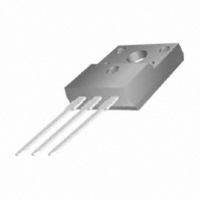
FDPF79N15 Fairchild Semiconductor, FDPF79N15 Datasheet

FDPF79N15
Specifications of FDPF79N15
Available stocks
Related parts for FDPF79N15
FDPF79N15 Summary of contents
Page 1
... Thermal Resistance, Case-to-Sink Typ. θCS R Thermal Resistance, Junction-to-Ambient θJA ©2007 Fairchild Semiconductor Corporation FDP79N15 / FDPF79N15 Rev. B Description = 10 V These N-Channel enhancement mode power field effect transistors are produced using Fairchild’s proprietary, planar stripe, DMOS technology. This advanced technology has been especially tailored to ...
Page 2
... Starting ≤ 79A, di/dt ≤ 200A/μs, V ≤ Starting DSS 4. Pulse Test: Pulse width ≤ 300μs, Duty Cycle ≤ Essentially Independent of Operating Temperature Typical Characteristics FDP79N15 / FDPF79N15 Rev. B Package Reel Size TO-220 - TO-220F - T = 25°C unless otherwise noted C Conditions 250μ ...
Page 3
... I , Drain Current [A] D Figure 5. Capacitance Characteristics 6000 C 5000 oss 4000 C iss 3000 2000 C rss 1000 Drain-Source Voltage [V] DS FDP79N15 / FDPF79N15 Rev. B Figure 2. Transfer Characteristics Notes : 1. 250 μ s Pulse Test Figure 4. Body Diode Forward Voltage Variation vs. Source Current 20V Note : T ...
Page 4
... V , Drain-Source Voltage [V] DS Figure 10. Maximum Drain Current vs. Case Temperature Case Temperature [ C FDP79N15 / FDPF79N15 Rev. B (Continued) Figure 8. On-Resistance Variation 3.0 2.5 2.0 1.5 1.0 * Notes : 0 250 μ 0.0 100 150 200 -100 o C] Figure 9-2. Maximum Safe Operating Area 10 μ s 100 μ ...
Page 5
... Typical Performance Characteristics Figure 11-1. Transient Thermal Response Curve for FDP79N15 10 10 Figure 11-2. Transient Thermal Response Curve for FDPF79N15 FDP79N15 / FDPF79N15 Rev. B (Continued) D=0.5 -1 0.2 0.1 0.05 0.02 * Notes : - 0.01 2. Duty Factor, D single pulse - Square Wave Pulse Duration [sec] 1 D=0 ...
Page 6
... Unclamped Inductive Switching Test Circuit & Waveforms FDP79N15 / FDPF79N15 Rev. B Gate Charge Test Circuit & Waveform Resistive Switching Test Circuit & Waveforms 6 www.fairchildsemi.com ...
Page 7
... FDP79N15 / FDPF79N15 Rev. B Peak Diode Recovery dv/dt Test Circuit & Waveforms 7 www.fairchildsemi.com ...
Page 8
... Mechanical Dimensions 9.90 (8.70) ø3.60 1.27 ±0.10 2.54TYP [2.54 ] ±0.20 10.00 FDP79N15 / FDPF79N15 Rev. B TO-220 ±0.20 ±0.10 1.52 ±0.10 0.80 ±0.10 2.54TYP [2.54 ] ±0.20 ±0.20 8 4.50 ±0.20 +0.10 1.30 –0.05 +0.10 0.50 2.40 ±0.20 –0.05 Dimensions in Millimeters www.fairchildsemi.com ...
Page 9
... Mechanical Dimensions MAX1.47 0.80 ±0.10 0.35 ±0.10 2.54TYP [2.54 ] ±0.20 FDP79N15 / FDPF79N15 Rev. B (Continued) TO-220F 10.16 ø3.18 ±0.20 ±0.10 (7.00) (1.00x45°) #1 2.54TYP [2.54 ] ±0.20 9.40 ±0.20 9 2.54 ±0.20 (0.70) +0.10 0.50 2.76 ±0.20 –0.05 Dimensions in Millimeters www.fairchildsemi.com ...
Page 10
... Definition of Terms Datasheet Identification Product Status Advance Information Formative or In Design Preliminary First Production No Identification Needed Full Production Obsolete Not In Production FDP79N15 / FDPF79N15 Rev. B HiSeC™ PowerSaver™ ® i-Lo™ PowerTrench ImpliedDisconnect™ Programmable Active Droop™ ® IntelliMAX™ QFET ISOPLANAR™ ...


