IRF7805A International Rectifier, IRF7805A Datasheet - Page 2
IRF7805A
Manufacturer Part Number
IRF7805A
Description
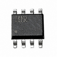
MOSFET N-CH 30V 13A 8-SOIC
Manufacturer
International Rectifier
Series
HEXFET®r
Datasheet
1.IRF7805TR.pdf
(5 pages)
Specifications of IRF7805A
Fet Type
MOSFET N-Channel, Metal Oxide
Fet Feature
Standard
Rds On (max) @ Id, Vgs
11 mOhm @ 7A, 4.5V
Drain To Source Voltage (vdss)
30V
Vgs(th) (max) @ Id
3V @ 250µA
Gate Charge (qg) @ Vgs
31nC @ 5V
Power - Max
2.5W
Mounting Type
Surface Mount
Package / Case
8-SOIC (3.9mm Width)
Lead Free Status / RoHS Status
Contains lead / RoHS non-compliant
Current - Continuous Drain (id) @ 25° C
-
Other names
*IRF7805A
Available stocks
Company
Part Number
Manufacturer
Quantity
Price

Part Number:
IRF7805A
Manufacturer:
IR
Quantity:
20 000
Company:
Part Number:
IRF7805APBF
Manufacturer:
IR
Quantity:
3 301
Company:
Part Number:
IRF7805ATR
Manufacturer:
IR
Quantity:
3 597
Company:
Part Number:
IRF7805ATRPBF
Manufacturer:
International Rectifier
Quantity:
1 810
Part Number:
IRF7805ATRPBF
Manufacturer:
IR
Quantity:
20 000


IRF7805
Notes:
‚
ƒ
„
…
†
2
BV
R
V
I
I
Q
Q
Q
R
t
t
t
t
I
I
V
Q
Q
Static @ T
Diode Characteristics
DSS
GSS
d(on)
r
d(off)
f
S
SM
DS(on)
GS(th)
G
SD
g
sw
oss
rr
rr(s)
Q
Q
Q
DSS
gs1
gs2
gd
Repetitive rating; pulse width limited by max. junction temperature.
Pulse width ≤ 300 µs; duty cycle ≤ 2%.
When mounted on 1 inch square copper board, t < 10 sec.
Typ = measured - Q
R
Devices are 100% tested to these parameters.
θ
is measured at T
Drain-to-Source Breakdown Voltage
Static Drain-to-Source On-Resistance
Gate Threshold Voltage
Drain-to-Source Leakage Current
Gate-to-Source Forward Leakage
Gate-to-Source Reverse Leakage
Total Gate Charge
Pre-Vth Gate-to-Source Charge
Post-Vth Gate-to-Source Charge
Gate-to-Drain Charge
Switch Charge (Q
Output Charge
Gate Resistance
Turn-On Delay Time
Rise Time
Turn-Off Delay Time
Fall Time
Continuous Source Current
(Body Diode)
Pulsed Source Current
(Body Diode)
Diode Forward Voltage
Reverse Recovery Charge
Reverse Recovery Charge
(with Parallel Schottky)
J
= 25°C (unless otherwise specified)
Parameter
J
oss
of approximately 90°C.
Ù
Parameter
gs2
+ Q
f
gd
)
f
Min. Typ. Max. Units
Min. Typ. Max. Units
–––
–––
–––
–––
–––
–––
–––
–––
–––
–––
–––
–––
–––
–––
–––
–––
–––
–––
–––
–––
–––
1.0
0.5
30
–––
–––
–––
–––
–––
–––
–––
–––
–––
–––
–––
9.2
3.7
1.4
6.8
8.2
3.0
22
16
20
38
16
88
55
-100
11.5
–––
150
100
–––
–––
–––
–––
–––
–––
–––
106
–––
–––
3.0
3.6
1.7
2.5
1.2
11
70
10
31
mΩ
µA
nA
nC
nC
nC
ns
ns
Ω
V
V
A
V
V
V
V
V
V
V
V
V
V
V
I
V
V
I
R
Resistive Load
MOSFET symbol
showing the
integral reverse
p-n junction diode.
T
di/dt = 700A/µs
V
di/dt = 700A/µs (with 10BQ040)
V
D
D
J
GS
GS
DS
DS
DS
DS
GS
GS
GS
DS
DS
DD
DS
DS
G
= 7.0A
= 7.0A
= 2Ω
= 25°C, I
= 0V, I
= 4.5V, I
= V
= 30V, V
= 24V, V
= 24V, V
= 12V
= -12V
= 5.0V
= 16V
= 16V, V
= 16V, V
= 16V, V
= 16V, V
GS
, I
D
Conditions
Conditions
D
S
= 250µA
D
GS
GS
GS
GS
GS
= 250µA
GS
GS
= 7.0A, V
= 7.0A
= 0V
= 0V
= 0V, T
= 0V
= 4.5V
= 0V, I
= 0V, I
www.irf.com
d
e
GS
J
S
S
= 100°C
= 7.0A
= 7.0A
= 0V
Related parts for IRF7805A
Image
Part Number
Description
Manufacturer
Datasheet
Request
R

Part Number:
Description:
SCHOTTKY RECTIFIER
Manufacturer:
International Rectifier Corp.
Datasheet:
Part Number:
Description:
SCHOTTKY RECTIFIER
Manufacturer:
International Rectifier Corp.
Datasheet:
Part Number:
Description:
SCHOTTKY RECTIFIER
Manufacturer:
International Rectifier Corp.
Datasheet:
Part Number:
Description:
SCHOTTKY RECTIFIER
Manufacturer:
International Rectifier Corp.
Datasheet:
Part Number:
Description:
SCHOTTKY RECTIFIER
Manufacturer:
International Rectifier Corp.
Datasheet:
Part Number:
Description:
SCHOTTKY RECTIFIER
Manufacturer:
International Rectifier Corp.
Datasheet:
Part Number:
Description:
SCHOTTKY RECTIFIER
Manufacturer:
International Rectifier Corp.
Datasheet:
Part Number:
Description:
SCHOTTKY RECTIFIER
Manufacturer:
International Rectifier Corp.
Datasheet:
Part Number:
Description:
SCHOTTKY RECTIFIER
Manufacturer:
International Rectifier Corp.
Datasheet:
Part Number:
Description:
SCHOTTKY RECTIFIER
Manufacturer:
International Rectifier Corp.
Datasheet:
Part Number:
Description:
SCHOTTKY RECTIFIER
Manufacturer:
International Rectifier Corp.
Datasheet:
Part Number:
Description:
SCHOTTKY RECTIFIER
Manufacturer:
International Rectifier Corp.
Datasheet:
Part Number:
Description:
SCHOTTKY RECTIFIER
Manufacturer:
International Rectifier Corp.
Datasheet:
Part Number:
Description:
SCHOTTKY RECTIFIER
Manufacturer:
International Rectifier Corp.
Datasheet:
Part Number:
Description:
SCHOTTKY RECTIFIER
Manufacturer:
International Rectifier Corp.
Datasheet: