IRFP450 STMicroelectronics, IRFP450 Datasheet
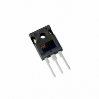
MOSFET N-CH 500V 14A TO-247

IRFP450

Manufacturer Part Number
IRFP450
Description
MOSFET N-CH 500V 14A TO-247
Manufacturer
STMicroelectronics
Series
PowerMESH™r
Datasheet

Specifications of IRFP450

Fet Type
MOSFET N-Channel, Metal Oxide
Fet Feature
Standard
Rds On (max) @ Id, Vgs
380 mOhm @ 7A, 10V
Drain To Source Voltage (vdss)
500V
Current - Continuous Drain (id) @ 25° C
14A
Vgs(th) (max) @ Id
4V @ 250µA
Gate Charge (qg) @ Vgs
90nC @ 10V
Input Capacitance (ciss) @ Vds
2000pF @ 25V
Power - Max
190W
Mounting Type
Through Hole
Package / Case
TO-247-3
Lead Free Status / RoHS Status
Contains lead / RoHS non-compliant
Other names
497-2735-5

Available stocks

Company
Part Number
Manufacturer
Quantity
Price
Part Number:
IRFP450
Manufacturer:
IR
Quantity:
12 500
Part Number:
IRFP450
Manufacturer:
ST
0
Part Number:
IRFP450
Manufacturer:
IR
Quantity:
20 000
Part Number:
IRFP450
Quantity:
4 000
Part Number:
IRFP450
Quantity:
1 125
Company:
Part Number:
IRFP450
Quantity:
29
Company:
Part Number:
IRFP450
Quantity:
55 000
Company:
Part Number:
IRFP450
Quantity:
55 000
Part Number:
IRFP450-E
Manufacturer:
IR
Quantity:
5 225
Part Number:
IRFP4502C
Quantity:
5 510
Part Number:
IRFP4502C
Manufacturer:
PHI
Quantity:
5 510
Part Number:
IRFP450A
Manufacturer:
FAIRCHILD
Quantity:
3 600
Part Number:
IRFP450A
Manufacturer:
IR
Quantity:
20 000
Part Number:
IRFP450APBF
Manufacturer:
VISHAY/威世
Quantity:
20 000
Company:
Part Number:
IRFP450APBF
Quantity:
1 350
Company:
Part Number:
IRFP450APBF
Quantity:
5 000
DESCRIPTION
The PowerMESH
generation of MESH OVERLAY
finements introduced greatly improve the Ron*area
figure of merit while keeping the device at the lead-
ing edge for what concerns switching speed, gate
charge and ruggedness.
APPLICATIONS
ABSOLUTE MAXIMUM RATINGS
(•)Pulse width limited by safe operating area
May 2001
IRFP450
TYPICAL R
EXTREMELY HIGH dv/dt CAPABILITY
100% AVALANCHE TESTED
NEW HIGH VOLTAGE BENCHMARK
GATE CHARGE MINIMIZED
SWITCH MODE POWER SUPPLIES (SMPS)
HIGH CURRENT, HIGH SPEED SWITCHING
DC-AC CONVERTERS FOR WELDING
EQUIPMENT AND UNINTERRUPTIBLE
POWER SUPPLIES AND MOTOR DRIVE
Symbol
dv/dt(1)
I
V
DM
P
V
V
T
DGR
I
I
TOT
T
GS
stg
DS
D
D
TYPE
j
( )
Drain-source Voltage (V
Drain-gate Voltage (R
Gate- source Voltage
Drain Current (continuos) at T
Drain Current (pulsed)
Total Dissipation at T
Derating Factor
Peak Diode Recovery voltage slope
Storage Temperature
Max. Operating Junction Temperature
DS
(on) = 0.31
500V
V
II is the evolution of the first
DSS
< 0.38
R
DS(on)
C
™.
GS
Parameter
= 25°C
GS
= 20 k )
N-CHANNEL 500V - 0.31 - 14A TO-247
The layout re-
= 0)
C
C
= 25°C
= 100°C
14 A
I
D
(1)I
SD
INTERNAL SCHEMATIC DIAGRAM
14A, di/dt 100A/µs, V
PowerMesh™II MOSFET
TO-247
–65 to 150
DD
Value
500
500
±30
190
150
8.7
1.5
3.5
14
56
V
(BR)DSS
1
IRFP450
2
, T
3
j
T
JMAX.
W/°C
Unit
V/ns
°C
°C
W
V
V
V
A
A
A
1/8

Related parts for IRFP450

IRFP450 Summary of contents

Page 1

... May 2001 N-CHANNEL 500V - 0.31 - 14A TO-247 R I DS(on ™. The layout re- INTERNAL SCHEMATIC DIAGRAM Parameter = 25° 100° 25°C C (1)I 14A, di/dt 100A/µ IRFP450 PowerMesh™II MOSFET TO-247 Value 500 500 ±30 14 8.7 56 190 1.5 3.5 –65 to 150 150 (BR)DSS j JMAX ...

Page 2

... IRFP450 THERMAL DATA Rthj-case Thermal Resistance Junction-case Max Rthj-amb Thermal Resistance Junction-ambient Max T Maximum Lead Temperature For Soldering Purpose l AVALANCHE CHARACTERISTICS Symbol Avalanche Current, Repetitive or Not-Repetitive I AR (pulse width limited by T Single Pulse Avalanche Energy E AS (starting ° ELECTRICAL CHARACTERISTICS (TCASE = 25 °C UNLESS OTHERWISE SPECIFIED) ...

Page 3

... 10V 4 Test Conditions V = 400V 4 10V G GS (see test circuit, Figure 5) Test Conditions Min di/dt = 100A/µ 100V 150° (see test circuit, Figure 5) Thermal Impedance IRFP450 Typ. Max. Unit Min. Typ. Max. Unit Typ. Max. Unit 1.6 V 670 ns 6.7 µC 20 ...

Page 4

... IRFP450 Output Characteristics Transconductance Gate Charge vs Gate-source Voltage 4/8 Transfer Characteristics Static Drain-source On Resistance Capacitance Variations ...

Page 5

... Normalized Gate Thereshold Voltage vs Temp. Source-drain Diode Forward Characteristics Normalized On Resistance vs Temperature IRFP450 5/8 ...

Page 6

... IRFP450 Fig. 1: Unclamped Inductive Load Test Circuit Fig. 3: Switching Times Test Circuit For Resistive Load Fig. 5: Test Circuit For Inductive Load Switching And Diode Recovery Times 6/8 Fig. 2: Unclamped Inductive Waveform Fig. 4: Gate Charge test Circuit ...

Page 7

... IRFP450 DIM. MIN. A 4.85 D 2. 15.45 L 19. 14. Dia 3.55 7/8 TO-247 MECHANICAL DATA mm. TYP MAX. 5.15 2.60 0.80 1. 2.40 3.40 10.90 15.75 20.15 4.30 18.50 14.80 34.60 5.50 3 5º 60º 3.65 inch MIN. TYP. MAX. 0.19 0.20 0.08 ...

Page 8

... IRFP450 Information furnished is believed to be accurate and reliable. However, STMicroelectronics assumes no responsibility for the consequences of use of such information nor for any infringement of patents or other rights of third parties which may result from its use. No license is granted by implication or otherwise under any patent or patent rights of STMicroelectronics. Specification mentioned in this publication are subject to change without notice ...

Related keywords