STB80NF55-08-1 STMicroelectronics, STB80NF55-08-1 Datasheet
STB80NF55-08-1
Specifications of STB80NF55-08-1
Available stocks


Related parts for STB80NF55-08-1


STB80NF55-08-1 Summary of contents
Page 1
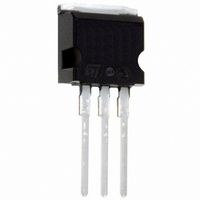
... Total Dissipation at T tot Derating Factor AS (1) E Single Pulse Avalanche Energy T Storage Temperature stg T Operating Junction Temperature j ( Pulse width limited by safe operating area. March 2005 . STB80NF55-08 STB80NF55-08-1 - 80A D STripFET™ II POWER MOSFET Figure 1: Package R I DS(on TO-263 therefore a Figure 2: Internal Schematic Diagram MARKING ...
Page 2
... STB80NF55-08/-1 STP80NF55-08 Table 4: THERMAL DATA Rthj-case Thermal Resistance Junction-case Rthj-amb Thermal Resistance Junction-ambient T Maximum Lead Temperature For Soldering Purpose l ELECTRICAL CHARACTERISTICS (T Table 5: OFF Symbol Parameter Drain-source V (BR)DSS Breakdown Voltage Zero Gate Voltage I DSS Drain Current (V GS Gate-body Leakage I GSS Current ( (*) ...
Page 3
... Source-drain Current (pulsed (*) V Forward On Voltage t Reverse Recovery Time rr Q Reverse Recovery Charge rr Reverse Recovery Current I RRM (*) Pulsed: Pulse duration = 300 µs, duty cycle 1 Pulse width limited by safe operating area. Figure 3: Safe Operating Area STB80NF55-08/-1 STP80NF55-08 Test Conditions 4 (Resistive Load, Figure 17 44V 10V ...
Page 4
... STB80NF55-08/-1 STP80NF55-08 Figure 5: Output Characteristics Figure 7: Transconductance Figure 9: Gate Charge vs Gate-source Voltage 4/12 Figure 6: Transfer Characteristics Figure 8: Static Drain-source On Resistance Figure 10: Capacitance Variations ...
Page 5
... Figure 11: Normalized Gate Threshold Voltage vs Temperature Figure 13: Source-drain Diode Forward Characteristics . . STB80NF55-08/-1 STP80NF55-08 Figure 12: Normalized on Resistance vs Temperature Figure 14: Normalized Breakdown Voltage vs Temperature 5/12 ...
Page 6
... STB80NF55-08/-1 STP80NF55-08 Figure 15: Unclamped Inductive Load Test Circuit Figure 17: Switching Times Test Circuits For Resis- tive Load Figure 19: Test Circuit For Inductive Load Switching And Diode Recovery Times 6/12 Figure 16: Unclamped Inductive Waveform Figure 18: Gate Charge test Circuit ...
Page 7
... STB80NF55-08/-1 STP80NF55-08 inch. TYP. TYP. 0.181 0.106 0.009 0.037 0.067 0.024 0.054 0.368 0.315 0.409 0.334 0.208 0.624 0.055 0.069 0.126 0.016 0° ...
Page 8
... STB80NF55-08/-1 STP80NF55-08 TO-262 (I DIM. MIN. A 4.4 A1 2.49 B 0.7 B2 1.14 C 0.45 C2 1.23 D 8. 13.1 L1 3.48 L2 1.27 L2 8/12 2 PAK) MECHANICAL DATA mm TYP. MAX. MIN. 4.6 0.173 2.69 0.098 0.93 0.027 1.7 0.044 0.6 0.017 1.36 0.048 9.35 0.352 2.7 0.094 10.4 0.393 13 ...
Page 9
... F1 1.14 F2 1.14 G 4.95 G1 2 13.0 L5 2.65 L6 15.25 L7 6.2 L9 3.5 DIA. 3.75 Dia STB80NF55-08/-1 STP80NF55-08 mm MAX. MIN. 4.60 0.173 1.32 0.048 2.72 0.094 1.27 0.70 0.019 0.88 0.024 1.70 0.044 1.70 0.044 5.15 0.194 2.7 0.094 10.40 0.393 16.4 14.0 ...
Page 10
... STB80NF55-08/-1 STP80NF55- PAK FOOTPRINT TAPE AND REEL SHIPMENT (suffix ”T4”)* TAPE MECHANICAL DATA mm DIM. MIN. MAX. MIN. A0 10.5 10.7 0.413 B0 15.7 15.9 0.618 D 1.5 1.6 0.059 D1 1.59 1.61 0.062 E 1.65 1.85 0.065 F 11.4 11.6 0.449 K0 4.8 5.0 0.189 P0 3.9 4.1 ...
Page 11
... Table 11: Revision History Date Revision 1.0 January 2005 STB80NF55-08/-1 STP80NF55-08 Description of Changes FIRST ISSUE 11/12 ...
Page 12
... STB80NF55-08/-1 STP80NF55-08 Information furnished is believed to be accurate and reliable. However, STMicroelectronics assumes no responsibility for the consequences of use of such information nor for any infringement of patents or other rights of third parties which may result from its use. No license is granted by implication or otherwise under any patent or patent rights of STMicroelectronics. Specifications mentioned in this publication are subject to change without notice ...