MTD2955VT4 ON Semiconductor, MTD2955VT4 Datasheet

MOSFET P-CH 60V 12A DPAK

MTD2955VT4

Manufacturer Part Number
MTD2955VT4
Description
MOSFET P-CH 60V 12A DPAK
Manufacturer
ON Semiconductor
Datasheet

Specifications of MTD2955VT4

Fet Type
MOSFET P-Channel, Metal Oxide
Fet Feature
Standard
Rds On (max) @ Id, Vgs
230 mOhm @ 6A, 10V
Drain To Source Voltage (vdss)
60V
Current - Continuous Drain (id) @ 25° C
12A
Vgs(th) (max) @ Id
4V @ 250µA
Gate Charge (qg) @ Vgs
30nC @ 10V
Input Capacitance (ciss) @ Vds
770pF @ 25V
Power - Max
60W
Mounting Type
Surface Mount
Package / Case
DPak, TO-252 (2 leads+tab), SC-63
Lead Free Status / RoHS Status
Contains lead / RoHS non-compliant
Other names
MTD2955VT4OS

Available stocks

Company
Part Number
Manufacturer
Quantity
Price
Part Number:
MTD2955VT4
Manufacturer:
ONSEMI
Quantity:
905
MTD2955V
Power MOSFET 12 A, 60 V
P−Channel DPAK
avalanche and commutation modes. Designed for low voltage, high
speed switching applications in power supplies, converters and power
motor controls, these devices are particularly well suited for bridge
circuits where diode speed and commutating safe operating areas are
critical and offer additional safety margin against unexpected voltage
transients.
Features
© Semiconductor Components Industries, LLC, 2006
August, 2006 − Rev. 8
MAXIMUM RATINGS
Stresses exceeding Maximum Ratings may damage the device. Maximum
Ratings are stress ratings only. Functional operation above the Recommended
Operating Conditions is not implied. Extended exposure to stresses above the
Recommended Operating Conditions may affect device reliability.
1. When surface mounted to an FR4 board using the minimum recommended
2. When surface mounted to an FR4 board using the 0.5 sq.in. pad size.
Drain−to−Source Voltage
Drain−to−Gate Voltage (R
Gate−to−Source Voltage
Drain Current − Continuous
Drain Current
Drain Current
Total Power Dissipation
Total Power Dissipation @ 25°C (Note 2)
Operating and Storage Temperature
Single Pulse Drain−to−Source Avalanche
Thermal Resistance
Maximum Lead Temperature for Soldering
This Power MOSFET is designed to withstand high energy in the
Avalanche Energy Specified
I
Pb−Free Packages are Available
DSS
− Continuous
− Non−repetitive (t
Derate above 25°C
Range
Energy − Starting T
(V
I
− Junction to Case
− Junction to Ambient (Note 1)
− Junction to Ambient (Note 2)
Purposes, 1/8″ from case for 10
seconds
pad size.
L
DD
= 12 Apk, L = 3.0 mH, R
and V
= 25 Vdc, V
DS(on)
− Continuous @ 100°C
− Single Pulse (t
Rating
GS
Specified at Elevated Temperature
p
J
≤ 10 ms)
= 10 Vdc, Peak
= 25°C
(T
GS
C
= 25°C unless otherwise noted)
G
= 1.0 MW)
p
= 25 W)
≤ 10 ms)
Symbol
T
V
V
V
R
R
R
V
J
E
I
P
DGR
GSM
, T
DSS
DM
T
I
I
qJC
qJA
qJA
GS
AS
D
D
D
L
stg
−55 to
Value
± 20
± 25
71.4
175
216
100
260
8.0
0.4
2.1
2.5
60
60
12
42
60
1
Watts
Watts
W/°C
°C/W
Unit
Vdc
Vdc
Vdc
Vpk
Adc
Apk
mJ
°C
°C
See detailed ordering and shipping information in the
package dimensions section on page 7 of this data sheet.
See general marking information in the device marking
section on page 7 of this data sheet.
DEVICE MARKING INFORMATION
R
ORDERING INFORMATION
DS(on)
1 2
1
2
G
3
http://onsemi.com
3
12 A, 60 V
= 185 mW (Typ)
4
4
P−Channel
Publication Order Number:
D
CASE 369C
CASE 369D
S
STYLE 2
STYLE 2
DPAK−3
DPAK−3
MTD2955V/D

Related parts for MTD2955VT4

MTD2955VT4 Summary of contents

Page 1

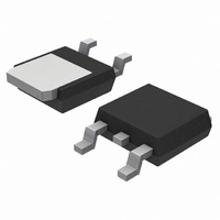
MTD2955V Power MOSFET P−Channel DPAK This Power MOSFET is designed to withstand high energy in the avalanche and commutation modes. Designed for low voltage, high speed switching applications in power supplies, converters and power motor controls, ...

Page 2

ELECTRICAL CHARACTERISTICS Characteristic OFF CHARACTERISTICS Drain−to−Source Breakdown Voltage ( Vdc 0.25 mAdc Temperature Coefficient (Positive) Zero Gate Voltage Drain Current ( Vdc Vdc Vdc, ...

Page 3

TYPICAL ELECTRICAL CHARACTERISTICS 25° DRAIN−TO−SOURCE VOLTAGE (VOLTS) DS Figure 1. On−Region Characteristics 0. ...

Page 4

Switching behavior is most easily modeled and predicted by recognizing that the power MOSFET is charge controlled. The lengths of various switching intervals (Dt) are determined by how fast the FET input capacitance can be charged by current from the ...

Page 5

TOTAL CHARGE (nC) T Figure 8. Gate−To−Source and Drain−To−Source Voltage versus Total Charge DRAIN−TO−SOURCE DIODE CHARACTERISTICS ...

Page 6

SINGLE PULSE T = 25° 100 1.0 R LIMIT DS(on) THERMAL LIMIT PACKAGE LIMIT 0.1 0.1 1 DRAIN−TO−SOURCE VOLTAGE (VOLTS) DS Figure 11. Maximum ...

Page 7

... ORDERING INFORMATION Device MTD2955V MTD2955VG MTD2955V−1 MTD2955V−1G MTD2955VT4 MTD2955VT4G †For information on tape and reel specifications, including part orientation and tape sizes, please refer to our Tape and Reel Packaging Specifications Brochure, BRD8011/D. DPAK−3 CASE 369C STYLE 2 Drain 1 Drain Gate Package DPAK− ...

Page 8

... 0.13 (0.005) M *For additional information on our Pb−Free strategy and soldering details, please download the ON Semiconductor Soldering and Mounting Techniques Reference Manual, SOLDERRM/D. PACKAGE DIMENSIONS DPAK−3 CASE 369C−01 ISSUE O SEATING −T− PLANE SOLDERING FOOTPRINT* 6.20 3.0 0.244 0.118 2.58 ...

Page 9

... American Technical Support: 800−282−9855 Toll Free USA/Canada Japan: ON Semiconductor, Japan Customer Focus Center 2−9−1 Kamimeguro, Meguro−ku, Tokyo, Japan 153−0051 Phone: 81−3−5773−3850 http://onsemi.com 9 NOTES: 1. DIMENSIONING AND TOLERANCING PER ANSI Y14.5M, 1982. 2. CONTROLLING DIMENSION: INCH. ...

Related keywords