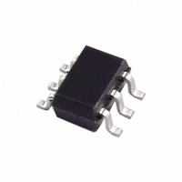
ADCMP601BKSZ-R2 Analog Devices Inc, ADCMP601BKSZ-R2 Datasheet - Page 8

ADCMP601BKSZ-R2
Manufacturer Part Number
ADCMP601BKSZ-R2
Description
Comparator Single R-R I/P 5.5V 6-Pin SC-70 T/R
Manufacturer
Analog Devices Inc
Type
with Latchr
Datasheet
1.ADCMP601BKSZ-REEL7.pdf
(16 pages)
Specifications of ADCMP601BKSZ-R2
Package
6SC-70
Typical Voltage Gain Range
70 to 90 dB
Rail To Rail
Rail to Rail Input
Number Of Channels Per Chip
1
Minimum Single Supply Voltage
2.5 V
Power Supply Type
Single
Number Of Elements
1
Output Type
CMOS, TTL
Voltage - Supply
2.5 V ~ 5.5 V
Mounting Type
Surface Mount
Package / Case
6-TSSOP, SC-88, SOT-363
Comparator Type
High Speed
No. Of Comparators
1
Response Time
3.5ns
Ic Output Type
CMOS, MOS, Open-Collector / Drain, TTL
Supply Current
3mA
Supply Voltage Range
2.5V To 5.5V
Rohs Compliant
Yes
Number Of Elements
1
Technology
CMOS
Input Offset Voltage
5mV
Input Bias Current (typ)
5uA
Single Supply Voltage (typ)
3/5V
Dual Supply Voltage (typ)
Not RequiredV
Supply Current (max)
4@5.5VmA
Power Supply Requirement
Single
Common Mode Rejection Ratio
50dB
Voltage Gain In Db
85dB
Power Supply Rejection Ratio
50dB
Single Supply Voltage (min)
2.5V
Single Supply Voltage (max)
5.5V
Dual Supply Voltage (min)
Not RequiredV
Dual Supply Voltage (max)
Not RequiredV
Power Dissipation
23mW
Operating Temp Range
-40C to 125C
Operating Temperature Classification
Automotive
Mounting
Surface Mount
Pin Count
6
Package Type
SC-70
Output Compatibility
CMOS, TTL
Lead Free Status / RoHS Status
Lead free / RoHS Compliant
Lead Free Status / RoHS Status
Lead free / RoHS Compliant
ADCMP600/ADCMP601/ADCMP602
TYPICAL PERFORMANCE CHARACTERISTICS
V
CCI
= V
–200
–400
–600
–800
–100
–150
800
600
400
200
150
100
–50
–10
–15
–20
CCO
50
20
15
10
–5
0
0
5
0
–1.0
Figure 8. Input Bias Current vs. Input Common Mode
–1
–1
= 2.5 V, T
V
CC
–0.5
Figure 6. LE/HYS Pin I/V Characteristics
= 2.5V
0
0
I
Figure 7. S
B
I
B
I
@ +125°C
B
@ +25°C
@ –40°C
0
A
1
1
COMMON-MODE VOLTAGE (V)
= 25°C, unless otherwise noted.
SHUTDOWN PIN VOLTAGE (V)
0.5
DN
V
V
CC
CC
Pin I/V Characteristics
2
2
= 2.5V
= 2.5V
LE/HYS (V)
1.0
3
3
1.5
4
4
2.0
V
V
CC
CC
5
5
2.5
= 5.5V
= 5.5V
6
6
3.0
3.5
7
7
Rev. A | Page 8 of 16
–10
–15
–20
250
200
150
100
450
400
350
300
250
200
150
100
50
20
15
10
–5
50
5
0
0
0
–1.0
50
0
V
CC
V
Figure 10. Hysteresis vs. R
–0.6
CC
= 2.5V
= 5.5V
Figure 11. Hysteresis vs. Pin Current
–0.2 0.2
150
Figure 9. V
–5
HYSTERESIS RESISTOR (kΩ)
250
0.6
OH
PIN CURRENT (µA)
/V
OL
1.0
I
OL
V
vs. Current Load
OUT
–10
350
VS V
HYS
1.4
(V)
I
OH
Control Resistor
OL
1.8
VS V
450
OH
2.2
–15
2.6
550
LOT 1
3.0
LOT 2
3.4
–20
650


