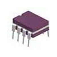
LM193AJ/883 National Semiconductor, LM193AJ/883 Datasheet - Page 7

LM193AJ/883
Manufacturer Part Number
LM193AJ/883
Description
Comparator Dual ±18V/36V 8-Pin CDIP Rail
Manufacturer
National Semiconductor
Specifications of LM193AJ/883
Package
8CDIP
Typical Response Time
1.3 us
Typical Response Time Range
0.5 to 5 us
Typical Voltage Gain Range
90 to 110 dB
Output Type
Open Collector
Number Of Channels Per Chip
2
Minimum Single Supply Voltage
2 V
Power Supply Type
Single|Dual
Number Of Elements
2
Technology
Bipolar
Input Offset Voltage
2mV
Input Bias Current (typ)
1nA
Response Time
1.3us
Single Supply Voltage (typ)
3/5/9/12/15/18/24/28V
Dual Supply Voltage (typ)
±3/±5/±9/±12/±15V
Supply Current (max)
1@5VmA
Power Supply Requirement
Single/Dual
Common Mode Rejection Ratio
60dB
Voltage Gain In Db
106.02dB
Power Supply Rejection Ratio
60dB
Single Supply Voltage (min)
2V
Single Supply Voltage (max)
36V
Dual Supply Voltage (min)
±1V
Dual Supply Voltage (max)
±18V
Power Dissipation
780mW
Operating Temp Range
-55C to 125C
Operating Temperature Classification
Military
Mounting
Through Hole
Pin Count
8
Package Type
CDIP
Lead Free Status / Rohs Status
Not Compliant
Available stocks
Company
Part Number
Manufacturer
Quantity
Price
Company:
Part Number:
LM193AJ/883
Manufacturer:
ZCOMM
Quantity:
1 400
Part Number:
LM193AJ/883
Manufacturer:
NS/国半
Quantity:
20 000
V
±I
t
RLH
IO
Symbol
Symbol
IB
LM193A - 100K Radiation Electrical Characteristics (Continued)
DC Drift Parameters
The following conditions apply, unless otherwise specified. +V = 5V, V
Delta calculations performed on QMLV devices at Group B, Subgroup 5 only
AC Parameters - Post Radiation Limits @ +25°C
The following conditions apply, unless otherwise specified. +V = 5V, V
Note 1: Absolute Maximum Ratings indicate limits beyond which damage to the device may occur. Operating Ratings indicate conditions for which the device is
functional, but do not guarantee specific performance limits. For guaranteed specifications and test conditions, see the Electrical Characteristics. The guaranteed
specifications apply only for the test conditions listed. Some performance characteristics may degrade when the device is not operated under the listed test
conditions.
Note 2: The maximum power dissipation must be derated at elevated temperatures and is dictated by T
junction to ambient thermal resistance), and T
θ
Note 3: The LM193A must be derated based on a 150°C, T
very small (P
Note 4: Short circuits from the output to V
current is approximately 20 mA independent of the magnitude of V
Note 5: This input current will only exist when the voltage at any of the input leads is driven negative. It is due to the collector-base junction of the input PNP
transistors becoming forward biased and thereby acting as input diode clamps. In addition to this diode action, there is also lateral NPN parasitic transistor action
on the IC chip. This transistor action can cause the output voltages of the comparators to go to the V
time duration that an input is driven negative. This is not destructive and normal output states will re-establish when the input voltage, which was negative, again
returns to a value greater than −0.3V
Note 6: Positive excursions of input voltage may exceed the power supply level. As long as the other voltage remains within the common-mode range, the
comparator will provide a proper output state. The low input voltage state must not be less than −0.3V (or 0.3V below the magnitude of the negative power supply,
if used).
Note 7: Human body model, 1.5KΩ in series with 100pF.
Note 8: Parameter guaranteed by the V
Note 9: Datalog reading in K = V/mV.
Note 10: The value for V
Note 11: Pre and post irradiation limits are identical to those listed under AC and DC electrical characteristics except as listed in the Post Radiation Limits Table.
These parts may be dose rate sensitive in a space environment and demonstrate enhanced low dose rate effect. Radiation end point limits for the noted parameters
are guaranteed only for the conditions as specified in MIL-STD-883, Method 1019
Note 12: Low dose rate testing has been performed on a wafer-by-wafer basis, per test method 1019 condition D of MIL-STD-883, with no enhanced low dose
rate sensitivity (ELDRS) effect.
JA
or the number given in the Absolute Maximum Ratings, whichever is lower.
D
Input Offset Voltage
Input Bias Current
Response Time
≤
100mV), provided the output transistors are allowed to saturate.
Diff
Parameter
Parameter
is not datalogged during Read and Record.
DC
.
IO
+
can cause excessive heating and eventual destruction. When considering short circuits to ground, the maximum output
tests.
A
(ambient temperature). The maximum allowable power dissipation at any temperature is P
+V = 30V
V
OD
Jmax
= 50mV
. The low bias dissipation and the ON-OFF characteristic of the outputs keep the chip dissipation
+
.
Conditions
Conditions
7
CM
CM
= 0V
= 0V
+
Notes
Notes
voltage level (or to ground for a large overdrive) for the
Jmax
(maximum junction temperature), θ
Min
-1.0
Min
-15
Max
Max
1.0
1.0
15
Unit
Unit
mV
nA
µS
Dmax
= (T
JA
www.national.com
(package
Jmax
groups
groups
- T
Sub-
Sub-
1
1
9
A
)/


