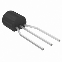
2N6028RLRA ON Semiconductor, 2N6028RLRA Datasheet - Page 3

2N6028RLRA
Manufacturer Part Number
2N6028RLRA
Description
THYRISTOR PROG UNIJUNCT 40V TO92
Manufacturer
ON Semiconductor
Datasheet
1.2N6028RLRAG.pdf
(6 pages)
Specifications of 2N6028RLRA
Voltage
40V
Power Dissipation (max)
300mW
Voltage - Output
11V
Voltage - Offset (vt)
600mV
Current - Gate To Anode Leakage (igao)
10nA
Current - Valley (iv)
25µA
Current - Peak
150nA
Package / Case
TO-92-3 (Standard Body), TO-226
Lead Free Status / RoHS Status
Contains lead / RoHS non-compliant
Other names
2N6028RLRAOSCT
Available stocks
Company
Part Number
Manufacturer
Quantity
Price
Company:
Part Number:
2N6028RLRAG
Manufacturer:
ON
Quantity:
2 000
*Indicates JEDEC Registered Data
4. Pulse Test: Pulse Width ≤ 300 ms, Duty Cycle ≤ 2%.
ELECTRICAL CHARACTERISTICS
Peak Current*
Offset Voltage*
Valley Current*
Gate to Anode Leakage Current*
Gate to Cathode Leakage Current
Forward Voltage*
Peak Output Voltage*
Pulse Voltage Rise Time
(V
(V
(V
(V
(V
(V
(V
(V
(V
(V
(I
(V
(V
Threshold
F
Turn−on
Figure 2. Peak Current (I
S
S
S
S
S
S
S
G
B
S
S
S
Adjust
V
= 50 mA Peak) (Note 4)
B
for
= 10 Vdc, R
= 10 Vdc, R
= 10 Vdc, R
= 10 Vdc, R
= 10 Vdc, R
= 10 Vdc, R
= 10 Vdc, R
= 20 Vdc, C
= 40 Vdc, T
= 40 Vdc, T
= 40 Vdc, Anode to Cathode Shorted)
= 20 Vdc, C
Scope
1A −
V
AK
I
Programmable Unijunction
with Program" Resistors
R1 and R2
A
100 k
1.0%
G
G
G
G
G
G
G
C
A
A
C
A
= 25°C, Cathode Open)
= 75°C, Cathode Open)
= 1 MW)
= 10 kW)
= 1 MW)
= 10 kW)
= 1 MW)
= 10 k W)
= 200 W)
= 0.2 mF)
= 0.2 mF)
20
K
+V
G
2N5270
Under
B
I
100 mV = 1.0 nA
0.01 mF
Test
P
Put
Characteristic
(SENSE)
+
−
R2
R1
− V
P
S
) Test Circuit
=
R1 + R2
(T
R1
R
V
(See Figure 1)
R
R
C
S
G
= 25°C unless otherwise noted)
= V
= R/2
Figure 1. Electrical Characterization
V
B
1B −
B/2
V
AK
I
Equivalent Test Circuit for
Figure 1A used for electrical
characteristics testing
(also see Figure 2)
A
+
(Both Types)
2N6027, 2N6028
http://onsemi.com
2N6027
2N6028
2N6027
2N6028
2N6027
2N6028
2N6027
2N6028
2N6027
2N6028
2N6027
2N6028
C
C
3
R
R
G
510 k
G
= R1 R2
Fig. No.
R1 + R2
2,9,11
1,4,5
1,6
3,7
V
1
−
−
3
S
+V
20 W
Figure 3. V
B
v
o
Symbol
I
I
I
GAO
GAO
16 k
27 k
GKS
V
V
V
I
I
t
P
V
r
o
T
F
o
and t
V
V
V
V
6.0 V
0.6 V
V
A
F
S
IC − Electrical Characteristics
V
I
o
P
+V
r
−V
Test Circuit
P
Min
0.2
0.2
0.2
1.5
1.0
6.0
70
25
−
−
−
−
−
−
−
−
−
−
−
V
T
t
f
= V
I
V
P
1.25
0.08
0.70
0.70
0.50
0.35
Typ
150
150
4.0
1.0
3.0
5.0
0.8
18
18
11
40
− V
−
−
S
I
Max
0.15
F
2.0
5.0
1.0
1.6
0.6
0.6
1.5
50
25
10
50
80
−
−
−
−
−
−
I
A
nAdc
nAdc
Unit
mA
mA
mA
ns
V
V
V
t


