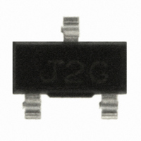
HSMS-2702-BLKG Avago Technologies US Inc., HSMS-2702-BLKG Datasheet - Page 8

HSMS-2702-BLKG
Manufacturer Part Number
HSMS-2702-BLKG
Description
DIODE SCHOTTKY 15V 350MA SOT-23
Manufacturer
Avago Technologies US Inc.
Datasheet
1.HSMS-2702-BLKG.pdf
(9 pages)
Specifications of HSMS-2702-BLKG
Diode Type
Schottky - 1 Pair Series Connection
Voltage - Peak Reverse (max)
15V
Current - Max
350mA
Capacitance @ Vr, F
6.7pF @ 0V, 1MHz
Power Dissipation (max)
350mW
Package / Case
SOT-23-3, TO-236-3, Micro3™, SSD3, SST3
Capacitance Ct
6.7pF
Diode Case Style
SOT-23
Series Resistance @ If
0.65ohm
Peak Reflow Compatible (260 C)
Yes
Leaded Process Compatible
Yes
Forward Voltage
550mV
Breakdown Voltage
15V
Rohs Compliant
Yes
Lead Free Status / RoHS Status
Lead free / RoHS Compliant
Resistance @ If, F
-
Lead Free Status / RoHS Status
Lead free / RoHS Compliant, Lead free / RoHS Compliant
Other names
516-1911
HSMS-2702-BLKG
HSMS-2702-BLKG
Available stocks
Company
Part Number
Manufacturer
Quantity
Price
Part Number:
HSMS-2702-BLKG
Manufacturer:
AVAGO/安华高
Quantity:
20 000
Because the automatic, pick-and-place equipment used
to assemble these products selects dice from adjacent
sites on the wafer, the two diodes which go into the
HSMS-2702 or HSMS-270C (series pair) are closely
matched —without the added expense of testing and
binning.
Current Handling in Clipping/Clamping Circuits
The purpose of a clipping/clamping diode is to handle
high currents, protecting delicate circuits downstream
of the diode. Current handling capacity is determined
by two sets of characteristics, those of the chip or device
itself and those of the package into which it is mounted.
Figure 8. Two Schottky Diodes Are Used for Clipping/Clamping in a Circuit.
Consider the circuit shown in Figure 8, in which two
Schottky diodes are used to protect a circuit from noise
spikes on a stream of digital data. The ability of the diodes
to limit the voltage spikes is related to their ability to sink
the associated current spikes. The importance of current
handling capacity is shown in Figure 9, where the forward
voltage generated by a forward current is compared in
two diodes.
Figure 9. Comparison of Two Diodes.
The first is a conventional Schottky diode of the type
generally used in RF circuits, with an R
second is a Schottky diode of identical characteristics,
save the R
relatively high value of R
diode’s terminals to rise as current increases. The power
dissipated in the diode heats the junction, causing R
climb, giving rise to a runaway thermal condition. In the
second diode with low R
place and the voltage across the diode terminals is main-
8
noisy data-spikes
long cross-site cable
6
5
4
3
2
1
0
pull-down
(or pull-up)
0
S
I
F
of 1.0 Ω. For the conventional diode, the
– FORWARD CURRENT (mA)
0.1
current
limiting
0.2
R
R
s
s
0V
= 7.7
= 1.0
S
0.3
S
causes the voltage across the
voltage limited to
Vs + Vd
0V – Vd
, such heating does not take
Vs
0.4
0.5
S
of 7.7 Ω. The
S
to
tained at a low limit even at high values of current.
Maximum reliability is obtained in a Schottky diode when
the steady state junction temperature is maintained at or
below 150°C, although brief excursions to higher junction
temperatures can be tolerated with no significant impact
upon mean-time-to-failure, MTTF. In order to compute
the junction temperature, Equations (1) and (3) below
must be simultaneously solved.
where:
I
I
V
R
T
I
n = diode ideality factor
θ
lead)
T
Equation (1) describes the forward V-I curve of a Schottky
diode. Equation (2) provides the value for the diode’s satu-
ration current, which value is plugged into (1). Equation
(3) gives the value of junction temperature as a function
of power dissipated in the diode and ambient (lead)
temperature.
The key factors in these equations are: R
tance of the diode where heat is generated under high
current conditions; θ
the Schottky die; and θ
resistance.
R
and is the lowest of any Schottky diode available from
Avago. Chip thermal resistance is typically 40°C/W; the
thermal resistance of the iron-alloy-leadframe, SOT-23
package is typically 460°C/W; and the thermal resistance
of the copper-leadframe, SOT-323 package is typically
110°C/W. The impact of package thermal resistance on
the current handling capability of these diodes can be
seen in Figures 3 and 4. Here the computed values of
junction temperature vs. forward current are shown
S
O
F
J
S
A
S
F
JC
= saturation current
= forward current
= junction temperature
= saturation current at 25°C
= θ
= forward voltage
= series resistance
for the HSMS-270x family of diodes is typically 0.7 Ω
I
T
= ambient (diode lead) temperature
I
S
F
J
= thermal resistance from junction to case (diode
= I
= I
= V
package
0
S
F
I
F JC
e
298
11600 (V
T
+ θ
J
+ T
chip
2
n
A
nT J
e
F
–4060
– I
chip
F
R
, the chip thermal resistance of
package
S
–1
)
T
1
J
–
, or the package thermal
298
1
(1)
(2)
(3)
S
, the series resis-


