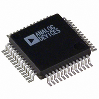
AD1835AASZ Analog Devices Inc, AD1835AASZ Datasheet - Page 13

AD1835AASZ
Manufacturer Part Number
AD1835AASZ
Description
Audio Codec 2ADC / 8DAC 24-Bit 52-Pin MQFP
Manufacturer
Analog Devices Inc
Type
General Purposer
Datasheet
1.AD1835AASZ.pdf
(24 pages)
Specifications of AD1835AASZ
Package
52MQFP
Adc/dac Resolution
24 Bit
Number Of Channels
2ADC /8 DAC
Sampling Rate
96 KSPS
Number Of Adcs
2
Number Of Dacs
8
Operating Supply Voltage
3.3|5 V
Data Interface
Serial
Resolution (bits)
24 b
Number Of Adcs / Dacs
2 / 8
Sigma Delta
Yes
S/n Ratio, Adcs / Dacs (db) Typ
105 / 108
Dynamic Range, Adcs / Dacs (db) Typ
105 / 108
Voltage - Supply, Analog
4.5 V ~ 5.5 V
Voltage - Supply, Digital
4.5 V ~ 5.5 V
Operating Temperature
-40°C ~ 85°C
Mounting Type
Surface Mount
Package / Case
52-BQFP
Lead Free Status / RoHS Status
Lead free / RoHS Compliant
For Use With
EVAL-AD1835AEB - BOARD EVALUATION FOR AD1835A
Lead Free Status / RoHS Status
Lead free / RoHS Compliant
Available stocks
Company
Part Number
Manufacturer
Quantity
Price
Company:
Part Number:
AD1835AASZ
Manufacturer:
ADI
Quantity:
30
Company:
Part Number:
AD1835AASZ
Manufacturer:
Analog Devices Inc
Quantity:
10 000
Company:
Part Number:
AD1835AASZ-REEL
Manufacturer:
Analog Devices Inc
Quantity:
10 000
The format is similar to the Motorola SPI format except the
input data-word is 16 bits wide. The maximum serial bit clock
frequency is 12.5 MHz and may be completely asynchronous
to the sample rate of the ADCs and DACs. Figure 3 shows the
format of the SPI signal.
Serial Data Ports—Data Format
The ADC serial data output mode defaults to the popular I
format, where the data is delayed by 1 BCLK interval from the
edge of the LRCLK. By changing Bits 6 to 8 in ADC Control
Register 2, the serial mode can be changed to right-justified
(RJ), left-justified DSP (DSP), or left-justified (LJ). In the
RJ mode, it is necessary to set Bits 4 and 5 to define the width
of the data-word.
The DAC serial data input mode defaults to I
Bits 5, 6, and 7 in DAC Control Register 1, the mode can be
changed to RJ, DSP, LJ, Packed Mode 1, or Packed Mode 2.
The word width defaults to 24 bits but can be changed by
reprogramming Bits 3 and 4 in DAC Control Register 1.
Packed Modes
The AD1835A has a packed mode that allows a DSP or other
controller to write to all DACs and read all ADCs using one input
data pin and one output data pin. Packed Mode 256 refers to
the number of BCLKs in each frame. The LRCLK is low while
data from a left channel DAC or ADC is on the data pin and
high while data from a right channel DAC or ADC is on the
REV. A
SDATA
SDATA
SDATA
SDATA
LRCLK
LRCLK
LRCLK
LRCLK
BCLK
BCLK
BCLK
BCLK
NOTES
1. DSP MODE DOES NOT IDENTIFY CHANNEL.
2. LRCLK NORMALLY OPERATES AT
3. BCLK FREQUENCY IS NORMALLY 64
MSB
MSB
MSB
MSB
LEFT CHANNEL
LEFT CHANNEL
LEFT CHANNEL
f
S
RIGHT-JUSTIFIED MODE – SELECT NUMBER OF BITS PER CHANNEL
EXCEPT FOR DSP MODE, WHICH IS 2
LRCLK BUT MAY BE OPERATED IN BURST MODE.
LEFT-JUSTIFIED MODE – 16 BITS TO 24 BITS PER CHANNEL
2
LSB
S. By changing
DSP MODE – 16 BITS TO 24 BITS PER CHANNEL
I
2
S MODE – 16 BITS TO 24 BITS PER CHANNEL
Figure 4. Stereo Serial Modes
LSB
LSB
2
S
LSB
–13–
1/f
S
data pin. DAC data is applied on the DSDATA1 pin and ADC
data is available on the ASDATA pin. Figures 7 to 12 show the
timing for the packed mode. Packed mode is available for 48 kHz
and 96 kHz.
Auxiliary (TDM) Mode
A special auxiliary mode is provided to allow three external stereo
ADCs to be interfaced to the AD1835A to provide 8-in/8-out
operation. In addition, this mode supports glueless interface to
a single SHARC DSP serial port, allowing a SHARC DSP to
access all eight channels of analog I/O. In this special mode,
many pins are redefined; see Table IV for a list of redefined pins.
The auxiliary and TDM interfaces are independently configurable
to operate as masters or slaves. When the auxiliary interface is
set as a master, by programming the auxiliary mode bit in
ADC Control Register 2, the AUXLRCLK and AUXBCLK
are generated by the AD1835A. When the auxiliary interface is
set as a slave, the AUXLRCLK and AUXBCLK need to be
generated by an external ADC as shown in Figure 15.
The TDM interface can be set to operate as a master or slave by
connecting the M/S pin to DGND or ODVDD, respectively. In
master mode, the FSTDM and BCLK signals are outputs and
are generated by the AD1835A. In slave mode, the FSTDM
and BCLK are inputs and should be generated by the SHARC.
Both 48 kHz and 96 kHz operations are available (based on a
12.288 MHz or 24.576 MHz MCLK) in this mode.
MSB
f
S
.
MSB
MSB
MSB
RIGHT CHANNEL
RIGHT CHANNEL
RIGHT CHANNEL
LSB
LSB
LSB
AD1835A
LSB


