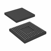
ADSP-BF533SBBC500 Analog Devices Inc, ADSP-BF533SBBC500 Datasheet - Page 16

ADSP-BF533SBBC500
Manufacturer Part Number
ADSP-BF533SBBC500
Description
DSP Fixed-Point 16-Bit 500MHz 500MIPS 160-Pin CSP-BGA
Manufacturer
Analog Devices Inc
Series
Blackfin®r
Type
Fixed Pointr
Datasheet
1.ADSP-BF531SBSTZ400.pdf
(12 pages)
Specifications of ADSP-BF533SBBC500
Package
160CSP-BGA
Numeric And Arithmetic Format
Fixed-Point
Maximum Speed
500 MHz
Device Million Instructions Per Second
500 MIPS
Rohs Status
RoHS non-compliant
Interface
SPI, SSP, UART
Clock Rate
500MHz
Non-volatile Memory
ROM (1 kB)
On-chip Ram
148kB
Voltage - I/o
1.8V, 2.5V, 3.3V
Voltage - Core
1.20V
Operating Temperature
-40°C ~ 85°C
Mounting Type
Surface Mount
Package / Case
160-CSPBGA
For Use With
ADZS-BFAUDIO-EZEXT - BOARD EVAL AUDIO BLACKFINADZS-BFAV-EZEXT - BOARD DAUGHT ADSP-BF533,37,61KITADZS-BF533-EZLITE - KIT W/BOARD EVAL FOR ADSP-BF533
Lead Free Status / RoHS Status
Available stocks
Company
Part Number
Manufacturer
Quantity
Price
Company:
Part Number:
ADSP-BF533SBBC500
Manufacturer:
ADI
Quantity:
210
Company:
Part Number:
ADSP-BF533SBBC500
Manufacturer:
Analog Devices Inc
Quantity:
10 000
ADSP-BF531/BF532/BF533
28.
29.
DESCRIPTION:
Reads from the scratchpad memory may return incorrect data under some conditions. The problem occurs when reads of scratchpad
memory are immediately followed by another read (of any location, including non-scratchpad locations), where the addresses being
accessed do not have the same least significant address bit. This means that one of the transfers has to be a byte access. The other access
has to be either a byte, 16-bit or 32-bit access on a different byte boundary than the first access. In addition, the instruction immediately
before the Scratchpad memory read has to generate a memory stall due to either a dual DAG bank collision, a non-L1 memory data fetch,
or a cache-line fill.
If an instruction does not perform a read immediately after the scratchpad read, no problems occur. Also, back to back non-byte reads
function properly.
WORKAROUND:
The simplest workaround for assembly programmers is to place any non-read instruction after each scratchpad read. For C programmers,
one solution is not to map any data to the scratchpad.
Alternatively the VisualDSP++ Blackfin compiler includes a workaround for this hardware anomaly. The compiler will automatically enable
the workaround for the appropriate silicon revisions and part numbers, or the workaround can be enabled manually by specifying the
compiler flag -workaround scratchpad-read' With the workaround enabled, when a sequence of three load instructions occurs (or occur
as parts of a multi-issue instruction), where at least one of (2) and (3) is a byte load, a nop will be inserted between (1) and (2) or (2) and (3):
A load instruction (1);
A load instruction (2);
A load instruction (3);
The macro __WORKAROUND_SCRATCHPAD_READ will be defined at compile, assemble and link stages when the workaround is enabled.
The VisualDSP++ run-time libraries also avoid this anomaly for appropriate silicon revisions and part numbers.
APPLIES TO REVISION(S):
0.3, 0.4
DESCRIPTION:
In this Boot Mode, the DMA5_CONFIG and SPI_CTL registers are not restored to their default (reset) states before executing the user's
application code. The DMA5 channel remains enabled in stop mode and the SPI remains enabled in RX DMA mode.
WORKAROUND:
The user's application must reset these registers before either the SPI or DMA channel 5 can be used.
APPLIES TO REVISION(S):
0.3, 0.4, 0.5, 0.6
05000227 - Scratchpad Memory Bank Reads May Return Incorrect Data:
05000229 - SPI Slave Boot Mode Modifies Registers from Reset Value:
NR003532D | Page 16 of 45 | July 2008
Silicon Anomaly List


