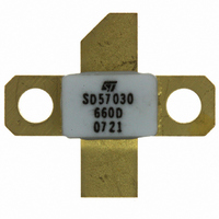
SD57030 STMicroelectronics, SD57030 Datasheet
SD57030
Specifications of SD57030
SD57030
Available stocks


Related parts for SD57030


SD57030 Summary of contents
Page 1
... The SD57030 is a common source N-channel enhancement-mode lateral Field-Effect RF power transistor designed for broadband commercial and industrial applications at frequencies up to 1.0 GHz. The SD57030 is designed for high gain and broadband performance operating in common source mode ideal for base station applications requiring high linearity. ...
Page 2
... Contents Contents 1 Electrical data . . . . . . . . . . . . . . . . . . . . . . . . . . . . . . . . . . . . . . . . . . . . . . 3 1.1 Maximum ratings . . . . . . . . . . . . . . . . . . . . . . . . . . . . . . . . . . . . . . . . . . . . 3 1.2 Thermal data . . . . . . . . . . . . . . . . . . . . . . . . . . . . . . . . . . . . . . . . . . . . . . . 3 2 Electrical characteristics . . . . . . . . . . . . . . . . . . . . . . . . . . . . . . . . . . . . . 4 2.1 Static . . . . . . . . . . . . . . . . . . . . . . . . . . . . . . . . . . . . . . . . . . . . . . . . . . . . . 4 2.2 Dynamic . . . . . . . . . . . . . . . . . . . . . . . . . . . . . . . . . . . . . . . . . . . . . . . . . . . 4 3 Typical performance (CW Test circuit . . . . . . . . . . . . . . . . . . . . . . . . . . . . . . . . . . . . . . . . . . . . . . . . . 6 5 Text circuit layout . . . . . . . . . . . . . . . . . . . . . . . . . . . . . . . . . . . . . . . . . . . 8 6 Package mechanical data . . . . . . . . . . . . . . . . . . . . . . . . . . . . . . . . . . . . . 9 7 Revision history . . . . . . . . . . . . . . . . . . . . . . . . . . . . . . . . . . . . . . . . . . . 10 2/11 SD57030 ...
Page 3
... SD57030 1 Electrical data 1.1 Maximum ratings Table 1. Absolute maximum ratings (T Symbol V (BR)DSS V DGR DISS Tj T STG 1.2 Thermal data Table 2. Thermal data Symbol R thJC CASE Parameter Drain-Source voltage Drain-Gate voltage ( MΩ) GS Gate-Source voltage Drain current Power dissipation (@ Tc = 70°C) Max. operating junction temperature ...
Page 4
... All phase angles 4/ Test conditions MHz MHz MHz DS Test conditions 945 MHz 945 MHz DQ OUT 945 MHz DQ OUT 945 MHz DQ OUT SD57030 Min Typ Max Unit 65 V µA 1 µA 1 2.0 5.0 V 1.3 V 1.8 mho 2.7 pF Min Typ Max Unit 10:1 VSWR ...
Page 5
... SD57030 3 Typical performance (CW) Figure 2. Output power vs input power 0.2 0.4 0.6 Pin, INPUT POWER (W) Figure 4. Output power vs gate source voltage 35 f= 945 MHz 30 Vdd Idq Vgs, GATE-SOURCE VOLTAGE (V) Figure 945 MHz Vdd Idq 0.8 1 1.2 1.4 Figure Typical performance (CW) Power gain and efficiency vs ...
Page 6
... Test circuit 4 Test circuit Figure 6. Test circuit schematic Dimensions at component symbols are reference for component placement. 2 Gap between ground & transmission line = 0.056 [1.42] +0.002 [0.05] -0.000 [0.00] typ. 3 Dimensions of input and output component from edge of transmission lines. 6/11 SD57030 + OUT ...
Page 7
... SD57030 Table 5. Test circuit component part list Component C19 C18, C14 C17 C16, C12, C11,C1 C15 C13 C9 C7, C6 FB2, FB1 L2, L1 PCB Description 200 µF / 63V ALLUMINIUM ELECTROLYTIC RADIAL LEAD CAPACITOR 0.1 µF / 500V SURFACE MOUNT CERAMIC CHIP CAPACITOR 100 pF ATC 100B SURFACE MOUNT CERAMIC CHIP CAPACITOR 47 pF ATC 100B SURFACE MOUNT CERAMIC CHIP CAPACITOR 10 µ ...
Page 8
... Text circuit layout 5 Text circuit layout Figure 7. Test fixture Figure 8. Test circuit photomaster 8/11 SD57030 SD57030 6.4 inches SD57030 ...
Page 9
... SD57030 6 Package mechanical data Table 6. M243 (.230 x .360 2L N/HERM W/FLG) mechanical data Dim Figure 9. Package dimensions Controlling dimension: Inches mm. Min Typ Max 5.21 5.72 5.46 6.48 5.59 6.10 14.27 20.07 20.57 8.89 9.40 0.10 0.15 3.18 4.45 1.83 2.24 1.27 1.78 ...
Page 10
... Revision history 7 Revision history Table 7. Document revision history Date 24-Mar-2003 11-Jul-2007 24-Aug-2007 10/11 Revision 5 First Issue. 6 Document reformatted, added lead free info 7 Cover page title updated SD57030 Changes ...
Page 11
... SD57030 Information in this document is provided solely in connection with ST products. STMicroelectronics NV and its subsidiaries (“ST”) reserve the right to make changes, corrections, modifications or improvements, to this document, and the products and services described herein at any time, without notice. All ST products are sold pursuant to ST’s terms and conditions of sale. ...