ATF-511P8-TR2 Avago Technologies US Inc., ATF-511P8-TR2 Datasheet
ATF-511P8-TR2
Specifications of ATF-511P8-TR2
Available stocks


Related parts for ATF-511P8-TR2


ATF-511P8-TR2 Summary of contents
Page 1
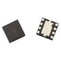
... LPCC Package Data Sheet Description Avago Technologies’s ATF-511P8 is a single-voltage high linearity, low noise E-pHEMT housed in an 8-lead JEDEC-standard leadless plastic chip carrier [3] (LPCC ) package. The device is ideal as a high linearity, low-noise, medium-power amplifier. Its operating frequency range is from 50 MHz to 6 GHz. ...
Page 2
... ATF-511P8 Absolute Maximum Ratings Symbol Parameter [2] V Drain–Source Voltage DS [2] V Gate–Source Voltage GS [2] V Gate Drain Voltage GD [2] I Drain Current DS I Gate Current GS [3] P Total Power Dissipation diss [ Input Power in max. T Channel Temperature CH T Storage Temperature STG θ [5] Thermal Resistance ...
Page 3
... ATF-511P8 Electrical Specifications T = 25°C, DC bias for RF parameters is Vds = 4.5V and Ids = 200 mA unless otherwise specified. A Symbol Parameter and Test Condition Vgs Operational Gate Voltage Vth Threshold Voltage Idss Saturated Drain Current Gm Transconductance Igss Gate Leakage Current [1] NF Noise Figure [1] G Gain ...
Page 4
Ohm 1.2 pF .02 λ RF Input Ohm 2.2 µF Gate DC Supply Figure 7. Simplified schematic of production test board. Primary purpose is to show 15 Ohm series resistor placement in gate supply. ...
Page 5
... ATF-511P8 Typical Performance Curves (at 25°C unless specified otherwise) Tuned for Optimal OIP3 at 4.5V 200 4 150 250 350 450 550 I DS (mA) Figure 8. OIP3 vs. I and GHz 4 150 250 350 450 550 I DS (mA) Figure 11. P1dB vs. and V at 900 MHz 4 150 250 350 ...
Page 6
... ATF-511P8 Typical Performance Curves, continued (at 25°C unless specified otherwise) Tuned for Optimal OIP3 at 4.5V, 200 -40 °C 25 °C 85 ° 0.5 1 1.5 2 2.5 3 3.5 4 FREQUENCY (GHz) Figure 17. P1dB vs. Temp and Freq. ATF-511P8 Typical Performance Curves (at 25°C unless specified otherwise) Tuned for Optimal P1dB at 4.5 V, 200 mA ...
Page 7
... ATF-511P8 Typical Performance Curves, continued (at 25°C unless specified otherwise) Tuned for Optimal P1dB at 4.5V, 200 4 150 250 350 450 550 I DS (mA) Figure 26. PAE vs. I and GHz -40 °C 25 ° °C 10 0.5 1 1.5 2 2.5 3 3.5 4 FREQUENCY (GHz) Figure 29. P1dB vs. Temp and Freq. ...
Page 8
... ATF-511P8 Typical Scattering Parameters, V Freq GHz Mag. Ang. dB 0.1 0.94 -134.9 31.16 0.2 0.93 -157.7 25.64 0.3 0.93 -166.6 22.26 0.4 0.93 -171.8 19.78 0.5 0.92 -173.9 18.70 0.6 0.93 -176.9 17.12 0.7 0.92 -178.8 15.78 0.8 0.93 178.7 14.61 0.9 ...
Page 9
... ATF-511P8 Typical Scattering Parameters, V Freq GHz Mag. Ang. dB 0.1 0.94 -132.6 31.26 0.2 0.93 -156.3 25.79 0.3 0.94 -165.6 22.40 0.4 0.93 -170.8 19.93 0.5 0.92 -173.1 18.84 0.6 0.92 -176.2 17.26 0.7 0.92 -178.2 15.92 0.8 0.92 179.4 14.76 0.9 ...
Page 10
... ATF-511P8 Typical Scattering Parameters, V Freq GHz Mag. Ang. dB 0.1 0.93 -125.4 30.99 0.2 0.93 -152.1 25.70 0.3 0.93 -162.8 22.34 0.4 0.92 -168.7 19.90 0.5 0.91 -170.8 18.78 0.6 0.91 -174.4 17.21 0.7 0.92 -176.8 15.88 0.8 0.92 -179.0 14.72 0.9 ...
Page 11
... ATF-511P8 Typical Scattering Parameters, V Freq GHz Mag. Ang. dB 0.1 0.94 -133.7 30.85 0.2 0.93 -156.9 25.31 0.3 0.93 -165.9 21.89 0.4 0.94 -170.9 19.48 0.5 0.93 -174.5 17.53 0.6 0.93 -175.8 16.77 0.7 0.93 -178.2 15.53 0.8 0.92 179.7 14.28 0.9 ...
Page 12
... ATF-511P8 Typical Scattering Parameters, V Freq GHz Mag. Ang. dB 0.1 0.95 -137.1 29.51 0.2 0.94 -159.0 23.89 0.3 0.94 -167.3 20.46 0.4 0.94 -172.0 18.04 0.5 0.93 -175.3 16.10 0.6 0.93 -176.8 15.36 0.7 0.93 -178.7 14.14 0.8 0.93 179.1 12.87 0.9 ...
Page 13
... Device Models Refer to Avago’s Web Site www.Avagotech.com/view/rf Ordering Information Part Number No. of Devices ATF-511P8-TR1 3000 ATF-511P8-TR2 10000 ATF-511P8-BLK 100 LPCC (JEDEC DFP-N) Package Dimensions D1 pin1 Bottom View Side View DIMENSIONS SYMBOL MIN. NOM. MAX. A 0.70 0.75 0. 0.02 0.05 A2 0.203 REF ...
Page 14
PCB Land Pattern and Stencil Design 2.80 (110.24) 0.70 (27.56) 0.25 (9.84) PIN 1 φ0.20 (7.87) Solder + mask 0.60 (23.62) RF transmission 0.80 (31.50) line 0.15 (5.91) 0.55 (21.65) PCB Land Pattern (top view) Notes: Typical stencil thickness is ...
Page 15
Tape Dimensions 10° Max A 0 DESCRIPTION CAVITY LENGTH WIDTH DEPTH PITCH BOTTOM HOLE DIAMETER PERFORATION DIAMETER PITCH POSITION CARRIER TAPE WIDTH THICKNESS COVER TAPE WIDTH TAPE THICKNESS DISTANCE CAVITY TO PERFORATION (WIDTH DIRECTION) CAVITY ...
Page 16
For product information and a complete list of distributors, please go to our web site: Avago, Avago Technologies, and the A logo are trademarks of Avago Technologies, Limited in the United States and other countries. Data subject to change. Copyright ...