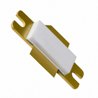
BLF6G27-135,112 NXP Semiconductors, BLF6G27-135,112 Datasheet - Page 3

BLF6G27-135,112
Manufacturer Part Number
BLF6G27-135,112
Description
IC WIMAX 2.7GHZ SOT502A
Manufacturer
NXP Semiconductors
Datasheet
1.BLF6G27LS-135118.pdf
(13 pages)
Specifications of BLF6G27-135,112
Package / Case
SOT502A
Transistor Type
LDMOS
Frequency
2.5GHz
Gain
16dB
Voltage - Rated
65V
Current Rating
34A
Current - Test
1.2A
Voltage - Test
32V
Power - Output
20W
Configuration
Single
Transistor Polarity
N-Channel
Resistance Drain-source Rds (on)
0.135 Ohms
Drain-source Breakdown Voltage
65 V
Gate-source Breakdown Voltage
13 V
Continuous Drain Current
34 A
Maximum Operating Temperature
+ 200 C
Mounting Style
SMD/SMT
Minimum Operating Temperature
- 65 C
Lead Free Status / RoHS Status
Lead free / RoHS Compliant
Noise Figure
-
Lead Free Status / RoHS Status
Lead free / RoHS Compliant, Lead free / RoHS Compliant
Other names
934061171112
BLF6G27-135
BLF6G27-135
BLF6G27-135
BLF6G27-135
NXP Semiconductors
6. Characteristics
7. Application information
BLF6G27-135_BLF6G27LS-135_2
Product data sheet
7.1 Ruggedness in class-AB operation
Table 6.
T
Table 7.
Mode of operation: 1-carrier N-CDMA, single carrier IS-95 with pilot, paging, sync and 6 traffic
channels (Walsh codes 8 to 13). PAR = 9.7 dB at 0.01 % probability on the CCDF, channel
bandwidth is 1.2288 MHz; f
V
circuit.
[1]
[2]
The BLF6G27-135 and BLF6G27LS-135 are capable of withstanding a load mismatch
corresponding to VSWR = 10 : 1 through all phases under the following conditions:
V
Symbol Parameter
V
V
I
I
I
g
R
C
Symbol
G
RL
ACPR
ACPR
P
DSS
DSX
GSS
j
DS
fs
DS
D
(BR)DSS
GS(th)
L(M)
DS(on)
rs
p
= 25 C unless otherwise specified.
in
= 32 V; I
Measured within 30 kHz bandwidth.
Measured at 2.7 GHz and 3 dB compression of the CCDF at 0.01 % probability.
= 28 V; I
885k
1980k
drain-source breakdown
voltage
gate-source threshold voltage
drain leakage current
drain cut-off current
gate leakage current
forward transconductance
drain-source on-state
resistance
feedback capacitance
Characteristics
Application information
Dq
Dq
Parameter
power gain
input return loss
drain efficiency
adjacent channel power ratio
(885 kHz)
adjacent channel power ratio
(1980 kHz)
peak output power
= 1200 mA; T
= 1200 mA; P
BLF6G27-135; BLF6G27LS-135
Rev. 02 — 26 May 2008
1
= 2500 MHz; f
case
L
= 25 C; unless otherwise specified, in a class-AB production
= P
L(1dB)
Conditions
V
V
I
V
V
V
V
V
V
I
V
f = 1 MHz
2
D
D
; f = 2700 MHz.
GS
DS
GS
GS
DS
GS
DS
GS
GS
= 2600 MHz; f
= 216 mA
= 7.2 A
= 10 V;
= 10 V
= 10 V; I
= 0 V; I
= 0 V; V
= V
= +11 V; V
= V
=0 V; V
Conditions
P
P
P
P
P
L(AV)
L(AV)
L(AV)
L(AV)
L(AV)
GS(th)
GS(th)
= 20 W
= 20 W
= 20 W
= 20 W
= 20 W
D
DS
DS
D
= 0.5 mA
+ 3.75 V;
+ 3.75 V;
= 6.3 A
= 28 V;
DS
= 28 V
3
= 2700 MHz; RF performance at
WiMAX power LDMOS transistor
= 0 V
[1]
[1]
[2]
Min
14
-
19.0
185
Min
65
1.4
-
30.6
-
-
-
-
48
65
Typ
16
22.5
200
Typ
-
2
-
34
-
12
0.085 0.135
3.15
© NXP B.V. 2008. All rights reserved.
10
52
67
Max
-
-
-
-
-
-
Max
-
2.4
4.2
-
420
-
-
3 of 13
Unit
V
V
A
nA
S
pF
Unit
dB
dB
%
dBc
dBc
W
A


