MCR12NG ON Semiconductor, MCR12NG Datasheet
MCR12NG
Specifications of MCR12NG
Available stocks


Related parts for MCR12NG

MCR12NG Summary of contents
Page 1
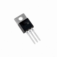
... I 2 °C T −40 to +125 J °C T −40 to +150 stg MCR12D MCR12DG MCR12M MCR12MG MCR12N MCR12NG Preferred devices are recommended choices for future use and best overall value. 1 http://onsemi.com SCRs 12 AMPERES RMS 400 thru 800 VOLTS MARKING DIAGRAM AY WW MCR12xG AKA TO−220AB CASE 221A− ...
Page 2
THERMAL CHARACTERISTICS Characteristic Thermal Resistance, Junction−to−Case Junction−to−Ambient Maximum Lead Temperature for Soldering Purposes 1/8″ from Case for 10 Seconds ELECTRICAL CHARACTERISTICS Characteristic OFF CHARACTERISTICS Peak Repetitive Forward or Reverse Blocking Current (V = Rated V and V ; Gate Open) ...
Page 3
MAXIMUM @ T = 25°C J MAXIMUM @ 0.1 0.5 1.0 1.5 2 INSTANTANEOUS ON−STATE VOLTAGE (VOLTS) T Figure 3. Typical On−State Characteristics 100 10 1 −40 −25 − ...
Page 4
... American Technical Support: 800−282−9855 Toll Free USA/Canada Japan: ON Semiconductor, Japan Customer Focus Center 2−9−1 Kamimeguro, Meguro−ku, Tokyo, Japan 153−0051 Phone: 81−3−5773−3850 http://onsemi.com 4 NOTES: 1. DIMENSIONING AND TOLERANCING PER ANSI Y14.5M, 1982. 2. CONTROLLING DIMENSION: INCH. ...