110RKI40 Vishay, 110RKI40 Datasheet - Page 2
110RKI40
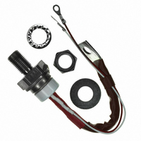
Manufacturer Part Number
110RKI40
Description
SCR 400V 110A TO-94
Manufacturer
Vishay
Datasheet
1.110RKI40.pdf
(7 pages)
Specifications of 110RKI40
Scr Type
Standard Recovery
Voltage - Off State
400V
Voltage - Gate Trigger (vgt) (max)
2V
Voltage - On State (vtm) (max)
1.57V
Current - On State (it (av)) (max)
110A
Current - On State (it (rms)) (max)
172A
Current - Gate Trigger (igt) (max)
120mA
Current - Hold (ih) (max)
200mA
Current - Off State (max)
20mA
Current - Non Rep. Surge 50, 60hz (itsm)
2080A, 2180A
Operating Temperature
-40°C ~ 140°C
Mounting Type
Chassis, Stud Mount
Package / Case
TO-209AC, TO-94
Current - On State (it (rms) (max)
172A
Breakover Current Ibo Max
2180 A
Rated Repetitive Off-state Voltage Vdrm
400 V
Off-state Leakage Current @ Vdrm Idrm
10 mA
Forward Voltage Drop
1.57 V
Gate Trigger Voltage (vgt)
2 V
Maximum Gate Peak Inverse Voltage
20 V
Gate Trigger Current (igt)
120 mA
Holding Current (ih Max)
200 mA
Mounting Style
Stud
Peak Repetitive Off-state Voltage, Vdrm
400V
Gate Trigger Current Max, Igt
100mA
Current It Av
110A
On State Rms Current It(rms)
172A
Peak Non Rep Surge Current Itsm 50hz
2.08kA
Lead Free Status / RoHS Status
Contains lead / RoHS non-compliant
Other names
*110RKI40


110/111RKI Series
Vishay High Power Products
www.vishay.com
2
ABSOLUTE MAXIMUM RATINGS
PARAMETER
Maximum average on-state current
at case temperature
Maximum RMS on-state current
Maximum peak, one-cycle
non-repetitive surge current
Maximum I
Maximum I
Low level value of threshold voltage
High level value of threshold voltage
Low level value of on-state slope resistance
High level value of on-state slope resistance
Maximum on-state voltage
Maximum holding current
Typical latching current
SWITCHING
PARAMETER
Maximum non-repetitive rate of rise
of turned-on current
Typical delay time
Typical turn-off time
BLOCKING
PARAMETER
Maximum critical rate of rise
of off-state voltage
Maximum peak reverse and
off-state leakage current
2
2
t for fusing
√t for fusing
For technical questions, contact: ind-modules@vishay.com
SYMBOL
SYMBOL
SYMBOL
V
V
I
T(RMS)
dV/dt
I
I
dI/dt
I
I
T(TO)1
T(TO)2
V
RRM
T(AV)
I
DRM
TSM
Phase Control Thyristors
I
2
r
r
t
t
I
I
2
TM
t1
t2
H
d
q
√t
L
t
(Stud Version), 110 A
,
Gate drive 20 V, 20 Ω, t
T
Gate current 1 A, dI
V
I
V
T
T
180° conduction, half sine wave
DC at 83 °C case temperature
t = 10 ms
t = 8.3 ms
t = 10 ms
t = 8.3 ms
t = 10 ms
t = 8.3 ms
t = 10 ms
t = 8.3 ms
t = 0.1 to 10 ms, no voltage reapplied
(16.7 % x π x I
(I > π x I
(16.7 % x π x I
(I > π x I
I
T
TM
pk
J
J
d
R
J
J
= T
= 0.67 % V
= T
= T
= 25 °C, anode supply 6 V resistive load
= 350 A, T
= 50 V, dV/dt = 20 V/µs; gate 0 V 25 Ω
= 50 A, T
J
J
J
maximum linear to 80 % rated V
maximum, anode voltage ≤ 80 % V
maximum, rated V
T(AV)
T(AV)
), T
), T
J
J
DRM
No voltage
reapplied
100 % V
reapplied
No voltage
reapplied
100 % V
reapplied
= T
T(AV)
T(AV)
= T
J
J
TEST CONDITIONS
TEST CONDITIONS
TEST CONDITIONS
= T
= T
J
, T
J
maximum, dI/dt = - 5 A/µs,
< I < π x I
< I < π x I
g
maximum, t
J
/dt = 1 A/µs
J
J
= 25 °C
maximum
maximum
RRM
RRM
r
≤ 1 µs
DRM
T(AV)
T(AV)
Sinusoidal half wave,
initial T
/V
p
RRM
= 10 ms sine pulse
), T
), T
applied
J
J
J
= T
= T
= T
DRM
J
J
J
DRM
maximum
maximum
maximum
Document Number: 93692
VALUES
VALUES
VALUES
Revision: 06-Jun-08
2080
2180
1750
1830
21.7
19.8
15.3
14.0
0.82
1.02
2.16
1.70
1.57
300
110
500
110
172
217
200
400
1.0
20
90
UNITS
UNITS
UNITS
kA
kA
V/µs
A/µs
mΩ
mA
mA
°C
µs
A
A
A
V
V
2
2
√s
s
Related parts for 110RKI40
Image
Part Number
Description
Manufacturer
Datasheet
Request
R

Part Number:
Description:
Phase Control Thyristors Stud Version , 110 A
Manufacturer:
Vishay
Datasheet:
Part Number:
Description:
357-036-542-201 CARDEDGE 36POS DL .156 BLK LOPRO
Manufacturer:
Vishay
Datasheet:
Part Number:
Description:
357-036-542-201 CARDEDGE 36POS DL .156 BLK LOPRO
Manufacturer:
Vishay
Datasheet:
Part Number:
Description:
357-036-542-201 CARDEDGE 36POS DL .156 BLK LOPRO
Manufacturer:
Vishay
Datasheet:
Part Number:
Description:
357-036-542-201 CARDEDGE 36POS DL .156 BLK LOPRO
Manufacturer:
Vishay
Datasheet:
Part Number:
Description:
357-036-542-201 CARDEDGE 36POS DL .156 BLK LOPRO
Manufacturer:
Vishay
Datasheet:
Part Number:
Description:
357-036-542-201 CARDEDGE 36POS DL .156 BLK LOPRO
Manufacturer:
Vishay
Datasheet:
Part Number:
Description:
357-036-542-201 CARDEDGE 36POS DL .156 BLK LOPRO
Manufacturer:
Vishay
Datasheet:
Part Number:
Description:
357-036-542-201 CARDEDGE 36POS DL .156 BLK LOPRO
Manufacturer:
Vishay
Datasheet:
Part Number:
Description:
357-036-542-201 CARDEDGE 36POS DL .156 BLK LOPRO
Manufacturer:
Vishay
Datasheet:
Part Number:
Description:
357-036-542-201 CARDEDGE 36POS DL .156 BLK LOPRO
Manufacturer:
Vishay
Datasheet:
Part Number:
Description:
357-036-542-201 CARDEDGE 36POS DL .156 BLK LOPRO
Manufacturer:
Vishay
Datasheet:
Part Number:
Description:
357-036-542-201 CARDEDGE 36POS DL .156 BLK LOPRO
Manufacturer:
Vishay
Datasheet:
Part Number:
Description:
357-036-542-201 CARDEDGE 36POS DL .156 BLK LOPRO
Manufacturer:
Vishay
Datasheet:
Part Number:
Description:
357-036-542-201 CARDEDGE 36POS DL .156 BLK LOPRO
Manufacturer:
Vishay
Datasheet: