ST333S04PFL0 Vishay, ST333S04PFL0 Datasheet - Page 3
ST333S04PFL0
Manufacturer Part Number
ST333S04PFL0
Description
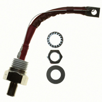
SCR PHASE CONT 400V 330A TO-118
Manufacturer
Vishay
Specifications of ST333S04PFL0
Scr Type
Standard Recovery
Voltage - Off State
400V
Voltage - Gate Trigger (vgt) (max)
3V
Voltage - On State (vtm) (max)
1.96V
Current - On State (it (av)) (max)
330A
Current - On State (it (rms)) (max)
518A
Current - Gate Trigger (igt) (max)
200mA
Current - Hold (ih) (max)
600mA
Current - Off State (max)
50mA
Current - Non Rep. Surge 50, 60hz (itsm)
11000A, 11500A
Operating Temperature
-40°C ~ 125°C
Mounting Type
Chassis, Stud Mount
Package / Case
TO-209AE, TO-118
Current - On State (it (rms) (max)
518A
Breakover Current Ibo Max
11520 A
Rated Repetitive Off-state Voltage Vdrm
400 V
Off-state Leakage Current @ Vdrm Idrm
50 mA
Forward Voltage Drop
1.96 V
Gate Trigger Voltage (vgt)
3 V
Maximum Gate Peak Inverse Voltage
5 V
Gate Trigger Current (igt)
200 mA
Holding Current (ih Max)
600 mA
Mounting Style
Stud
Peak Repetitive Off-state Voltage, Vdrm
400V
Gate Trigger Current Max, Igt
200mA
Current It Av
330A
On State Rms Current It(rms)
518A
Peak Non Rep Surge Current Itsm 50hz
11kA
Lead Free Status / RoHS Status
Lead free / RoHS Compliant
Other names
*ST333S04PFL0
VS-ST333S04PFL0
VS-ST333S04PFL0
VSST333S04PFL0
VSST333S04PFL0
VS-ST333S04PFL0
VS-ST333S04PFL0
VSST333S04PFL0
VSST333S04PFL0


Note
• The table above shows the increment of thermal resistance R
Document Number: 94409
Revision: 11-Aug-08
TRIGGERING
PARAMETER
Maximum peak gate power
Maximum average gate power
Maximum peak positive gate current
Maximum peak positive gate voltage
Maximum peak negative gate voltage
DC gate current required to trigger
DC gate voltage required to trigger
DC gate current not to trigger
DC gate voltage not to trigger
THERMAL AND MECHANICAL SPECIFICATIONS
PARAMETER
Maximum operating junction temperature range
Maximum storage temperature range
Maximum thermal resistance, junction to case
Maximum thermal resistance, case to heatsink
Mounting torque, ± 10 %
Approximate weight
Case style
ΔR
CONDUCTION ANGLE
thJC
CONDUCTION
180°
120°
90°
60°
30°
SINUSOIDAL CONDUCTION
For technical questions, contact: ind-modules@vishay.com
0.011
0.013
0.017
0.025
0.041
Phase Control Thyristors
SYMBOL
(Stud Version), 330 A
P
+ V
- V
P
V
V
I
G(AV)
I
I
GM
GT
GD
GM
GD
GT
GM
GM
SYMBOL
R
R
T
thC-hs
T
thJC
Stg
J
thJC
T
T
T
T
T
T
T
T
T
T
T
J
J
J
J
J
J
J
J
J
J
J
RECTANGULAR CONDUCTION
when devices operate at different conduction angles than DC
= T
= T
= T
= T
= - 40 °C
= 25 °C
= 125 °C
= - 40 °C
= 25 °C
= 125 °C
= T
J
J
J
J
J
DC operation
Mounting surface, smooth, flat and greased
Non-lubricated threads
See dimension - link at the end of datasheet
maximum, t
maximum, f = 50 Hz, d% = 50
maximum, t
maximum, t
maximum
TEST CONDITIONS
0.008
0.014
0.018
0.026
0.042
TEST CONDITIONS
p
p
p
≤ 5 ms
≤ 5 ms
≤ 5 ms
Maximum required gate trigger/
current/voltage are the lowest
value which will trigger all units
12 V anode to cathode applied
Maximum gate current/voltage
not to trigger is the maximum
value which will not trigger any
unit with rated V
cathode applied
Vishay High Power Products
DRM
ST330SPbF Series
TEST CONDITIONS
anode to
T
J
= T
J
maximum
TYP.
- 40 to 125
- 40 to 150
TO-209AE (TO-118)
200
100
2.5
1.8
1.1
50
VALUES
VALUES
(425)
0.10
0.03
48.5
535
10.0
0.25
2.0
3.0
5.0
20
10
www.vishay.com
MAX.
200
3
-
-
-
-
UNITS
(lbf · in)
K/W
UNITS
UNITS
N · m
K/W
mA
mA
°C
W
g
A
V
V
V
3
Related parts for ST333S04PFL0
Image
Part Number
Description
Manufacturer
Datasheet
Request
R

Part Number:
Description:
Inverter Grade Thyristors
Manufacturer:
Vishay
Datasheet:
Part Number:
Description:
357-036-542-201 CARDEDGE 36POS DL .156 BLK LOPRO
Manufacturer:
Vishay
Datasheet:
Part Number:
Description:
357-036-542-201 CARDEDGE 36POS DL .156 BLK LOPRO
Manufacturer:
Vishay
Datasheet:
Part Number:
Description:
357-036-542-201 CARDEDGE 36POS DL .156 BLK LOPRO
Manufacturer:
Vishay
Datasheet:
Part Number:
Description:
357-036-542-201 CARDEDGE 36POS DL .156 BLK LOPRO
Manufacturer:
Vishay
Datasheet:
Part Number:
Description:
357-036-542-201 CARDEDGE 36POS DL .156 BLK LOPRO
Manufacturer:
Vishay
Datasheet:
Part Number:
Description:
357-036-542-201 CARDEDGE 36POS DL .156 BLK LOPRO
Manufacturer:
Vishay
Datasheet:
Part Number:
Description:
357-036-542-201 CARDEDGE 36POS DL .156 BLK LOPRO
Manufacturer:
Vishay
Datasheet:
Part Number:
Description:
357-036-542-201 CARDEDGE 36POS DL .156 BLK LOPRO
Manufacturer:
Vishay
Datasheet:
Part Number:
Description:
357-036-542-201 CARDEDGE 36POS DL .156 BLK LOPRO
Manufacturer:
Vishay
Datasheet:
Part Number:
Description:
357-036-542-201 CARDEDGE 36POS DL .156 BLK LOPRO
Manufacturer:
Vishay
Datasheet:
Part Number:
Description:
357-036-542-201 CARDEDGE 36POS DL .156 BLK LOPRO
Manufacturer:
Vishay
Datasheet:
Part Number:
Description:
357-036-542-201 CARDEDGE 36POS DL .156 BLK LOPRO
Manufacturer:
Vishay
Datasheet:
Part Number:
Description:
357-036-542-201 CARDEDGE 36POS DL .156 BLK LOPRO
Manufacturer:
Vishay
Datasheet:
Part Number:
Description:
357-036-542-201 CARDEDGE 36POS DL .156 BLK LOPRO
Manufacturer:
Vishay
Datasheet: