12TTS08S Vishay, 12TTS08S Datasheet - Page 2
12TTS08S
Manufacturer Part Number
12TTS08S
Description
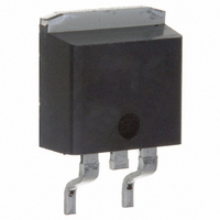
SCR PHASE CNTRL 800V 12A SMD-220
Manufacturer
Vishay
Datasheet
1.12TTS08S.pdf
(6 pages)
Specifications of 12TTS08S
Scr Type
Standard Recovery
Voltage - Off State
800V
Voltage - Gate Trigger (vgt) (max)
1V
Voltage - On State (vtm) (max)
1.2V
Current - On State (it (av)) (max)
8A
Current - On State (it (rms)) (max)
12.5A
Current - Gate Trigger (igt) (max)
15mA
Current - Hold (ih) (max)
30mA
Current - Off State (max)
1mA
Current - Non Rep. Surge 50, 60hz (itsm)
140A @ 50Hz
Operating Temperature
-40°C ~ 125°C
Mounting Type
Surface Mount
Package / Case
D²Pak, TO-263 (2 leads + tab)
Current - On State (it (rms) (max)
12.5A
Lead Free Status / RoHS Status
Contains lead / RoHS non-compliant
Other names
*12TTS08S
VS-12TTS08S
VS-12TTS08S
VS12TTS08S
VS12TTS08S
VS-12TTS08S
VS-12TTS08S
VS12TTS08S
VS12TTS08S


VS-12TTS08SPbF High Voltage Series
Vishay Semiconductors
www.vishay.com
2
ABSOLUTE MAXIMUM RATINGS
PARAMETER
Maximum average on-state current
Maximum RMS on-state current
Maximum peak one-cycle
non-repetitive surge current
Maximum I
Maximum I
Maximum on-state voltage drop
On-state slope resistance
Threshold voltage
Maximum reverse and direct leakage current
Typical holding current
Maximum latching current
Maximum rate of rise of off-state voltage
Maximum rate of rise of turned-on current
TRIGGERING
PARAMETER
Maximum peak gate power
Maximum average gate power
Maximum peak positive gate current
Maximum peak negative gate voltage
Maximum required DC gate current to trigger
Maximum required DC gate voltage to trigger
Maximum DC gate voltage not to trigger
Maximum DC gate current not to trigger
SWITCHING
PARAMETER
Typical turn-on time
Typical reverse recovery time
Typical turn-off time
2
2
t for fusing
√t for fusing
DiodesAmericas@vishay.com, DiodesAsia@vishay.com,
For technical questions within your region, please contact one of the following:
SYMBOL
SYMBOL
SYMBOL
I
I
RM
P
V
dV/dt
+ I
- V
T(RMS)
dI/dt
I
I
P
Phase Control SCR, 8 A
V
V
V
T(AV)
I
I
TSM
T(TO)
G(AV)
I
2
I
t
I
GT
GD
t
t
I
2
TM
r
GM
GD
/I
GT
gt
√t
H
L
rr
q
GM
t
GM
t
DM
T
T
T
10 ms sine pulse, rated V
10 ms sine pulse, no voltage reapplied, T
10 ms sine pulse, rated V
10 ms sine pulse, no voltage reapplied, T
t = 0.1 ms to 10 ms, no voltage reapplied, T
8 A, T
T
T
T
Anode supply = 6 V, resistive load, initial I
Anode supply = 6 V, resistive load
T
Anode supply = 6 V, resistive load, T
Anode supply = 6 V, resistive load, T
Anode supply = 6 V, resistive load, T
Anode supply = 6 V, resistive load, T
Anode supply = 6 V, resistive load, T
Anode supply = 6 V, resistive load, T
T
J
J
J
C
J
J
J
J
= 125 °C, V
= 25 °C
= 125 °C
= 125 °C
= 25 °C
= 125 °C
= 25 °C
= 108 °C, 180° conduction, half sine wave
J
= 25 °C
DRM
TEST CONDITIONS
TEST CONDITIONS
TEST CONDITIONS
V
R
= Rated value
= Rated V
DiodesEurope@vishay.com
RRM
RRM
RRM
applied, T
applied, T
/V
DRM
J
J
J
J
J
J
= - 65 °C
= 25 °C
= 125 °C
= - 65 °C
= 25 °C
= 125 °C
J
J
= 125 °C
J
= 125 °C
J
T
= 125 °C
= 125 °C
J
= 1 A
= 125 °C
Document Number: 94499
VALUES
VALUES
VALUES
1000
12.5
16.2
0.87
0.05
120
140
100
150
100
100
1.2
1.0
8.0
2.0
1.5
1.2
0.7
0.2
0.1
0.8
Revision: 08-Jun-10
72
30
50
10
20
15
10
3
8
1
UNITS
UNITS
UNITS
A
V/μs
A/μs
A
mΩ
mA
mA
mA
μs
W
2
A
A
V
V
V
V
2
√s
s
Related parts for 12TTS08S
Image
Part Number
Description
Manufacturer
Datasheet
Request
R

Part Number:
Description:
357-036-542-201 CARDEDGE 36POS DL .156 BLK LOPRO
Manufacturer:
Vishay
Datasheet:
Part Number:
Description:
357-036-542-201 CARDEDGE 36POS DL .156 BLK LOPRO
Manufacturer:
Vishay
Datasheet:
Part Number:
Description:
357-036-542-201 CARDEDGE 36POS DL .156 BLK LOPRO
Manufacturer:
Vishay
Datasheet:
Part Number:
Description:
357-036-542-201 CARDEDGE 36POS DL .156 BLK LOPRO
Manufacturer:
Vishay
Datasheet:
Part Number:
Description:
357-036-542-201 CARDEDGE 36POS DL .156 BLK LOPRO
Manufacturer:
Vishay
Datasheet:
Part Number:
Description:
357-036-542-201 CARDEDGE 36POS DL .156 BLK LOPRO
Manufacturer:
Vishay
Datasheet:
Part Number:
Description:
357-036-542-201 CARDEDGE 36POS DL .156 BLK LOPRO
Manufacturer:
Vishay
Datasheet:
Part Number:
Description:
357-036-542-201 CARDEDGE 36POS DL .156 BLK LOPRO
Manufacturer:
Vishay
Datasheet:
Part Number:
Description:
357-036-542-201 CARDEDGE 36POS DL .156 BLK LOPRO
Manufacturer:
Vishay
Datasheet:
Part Number:
Description:
357-036-542-201 CARDEDGE 36POS DL .156 BLK LOPRO
Manufacturer:
Vishay
Datasheet:
Part Number:
Description:
357-036-542-201 CARDEDGE 36POS DL .156 BLK LOPRO
Manufacturer:
Vishay
Datasheet:
Part Number:
Description:
357-036-542-201 CARDEDGE 36POS DL .156 BLK LOPRO
Manufacturer:
Vishay
Datasheet:
Part Number:
Description:
357-036-542-201 CARDEDGE 36POS DL .156 BLK LOPRO
Manufacturer:
Vishay
Datasheet:
Part Number:
Description:
357-036-542-201 CARDEDGE 36POS DL .156 BLK LOPRO
Manufacturer:
Vishay
Datasheet:
Part Number:
Description:
357-036-542-201 CARDEDGE 36POS DL .156 BLK LOPRO
Manufacturer:
Vishay
Datasheet: